Method for growing large-area graphene by utilizing multi-benzene-ring carbon source low-temperature chemical vapor deposition
A chemical vapor deposition, graphene technology, applied in graphene, nanotechnology for materials and surface science, gaseous chemical plating, etc. The effect of reduced consumption, fewer defects, good crystallinity
- Summary
- Abstract
- Description
- Claims
- Application Information
AI Technical Summary
Problems solved by technology
Method used
Image


Examples
Embodiment 1
[0063] Example 1: Low-temperature growth of large-area single-layer graphene from benzene liquid carbon source
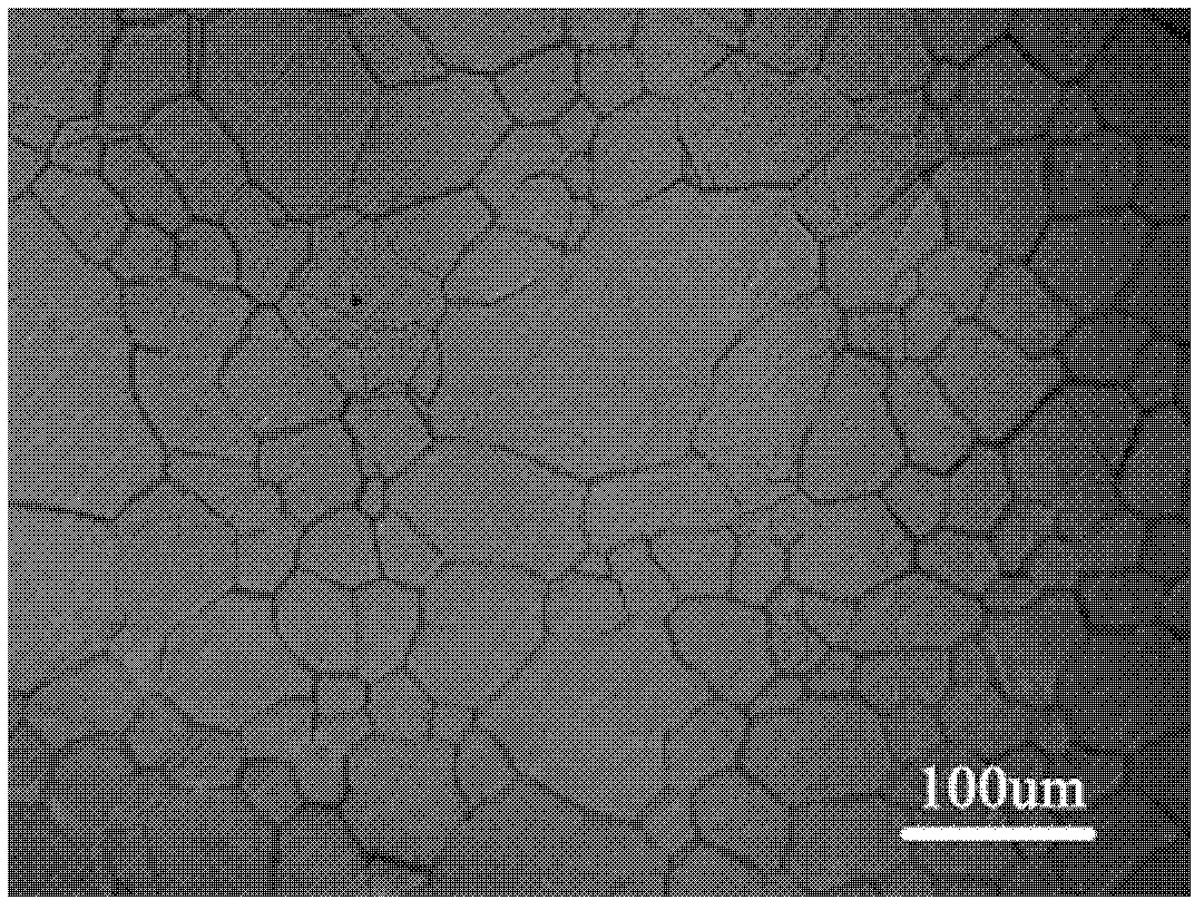
[0064] (1) Copper foil is used as the substrate, and the surface of the copper substrate is treated by mechanical polishing and electrochemical polishing successively to make the surface roughness below 50nm. The mechanical polishing speed is 800 rpm. The electrochemical workstation is used as the polishing power supply, the Ag / AgCl electrode is selected as the reference electrode, and the 85% phosphoric acid and polyethylene glycol mixture with a volume ratio of 3:1 is used as the electrochemical polishing solution; the copper foil to be polished is placed For the positive electrode, a copper sheet is used as the negative electrode; the electrochemical polishing voltage is 1-2V, and the polishing time is 1800s.
[0065] (2) After the electrochemical polishing, the copper foil was ultrasonically cleaned with acetone for 10 minutes, then ultrasonically cleaned with ...
Embodiment 2
[0072] Embodiment 2: Change the benzene liquid carbon source in embodiment 1 to 15 mg of naphthalene solid carbon source. The heating temperature of the naphthalene solid source during the graphene growth process is 80-120° C., and other processes are the same as in Example 1.
[0073] Example result: Figure 4 It is the Raman diagram of the graphene prepared under the condition of 600°C. The Raman test shows that the graphene has good crystallinity, and the peak intensity ratio of the 2D peak and the G peak is I 2D / I G is 1.9, and the D defect peak is very small; the crystallization properties of graphene prepared at 500°C and 700°C are basically the same. Figure 7It is the light transmittance test chart of graphene prepared under the condition of 600°C, indicating that the transmittance of graphene obtained by using naphthalene as a solid carbon source reaches 96.7%, which is a single-layer graphene; prepared under the conditions of 500°C and 700°C The transmittance of ...
Embodiment 3
[0074] Example 3: Change the benzene liquid carbon source in Example 1 to 15 mg of phenanthrene solid carbon source. The heating temperature of the phenanthrene solid source during the growth of graphene is 100-150° C., and other processes are the same as in Example 1.
[0075] Example result: Figure 4 It is the Raman diagram of the graphene prepared under the condition of 600°C. The Raman test shows that the graphene has good crystallinity, and the peak intensity ratio of the 2D peak and the G peak is I 2D / I G is 1.65, and the D defect peak is very small; the crystallization properties of graphene prepared at 500°C and 700°C are basically the same. Figure 8 It is the light transmittance test chart of graphene prepared at 600°C, indicating that the transmittance of graphene obtained by using phenanthrene as a solid carbon source reaches 96.5%, which is a single-layer graphene; prepared at 500°C and 700°C The transmittance of the obtained graphene is basically the same. ...
PUM
| Property | Measurement | Unit |
|---|---|---|
| surface roughness | aaaaa | aaaaa |
| thickness | aaaaa | aaaaa |
| thickness | aaaaa | aaaaa |
Abstract
Description
Claims
Application Information
 - Generate Ideas
- Intellectual Property
- Life Sciences
- Materials
- Tech Scout
- Unparalleled Data Quality
- Higher Quality Content
- 60% Fewer Hallucinations
Browse by: Latest US Patents, China's latest patents, Technical Efficacy Thesaurus, Application Domain, Technology Topic, Popular Technical Reports.
© 2025 PatSnap. All rights reserved.Legal|Privacy policy|Modern Slavery Act Transparency Statement|Sitemap|About US| Contact US: help@patsnap.com