Epitaxial wafer for light emitting diode
A technology for light-emitting diodes and epitaxial wafers, which is used in coatings, gaseous chemical plating, semiconductor devices, etc., can solve problems such as inability to apply long-wavelength technology, and achieve the effects of suppressing defects, high output power, and high efficiency
- Summary
- Abstract
- Description
- Claims
- Application Information
AI Technical Summary
Problems solved by technology
Method used
Image
Examples
Embodiment 1
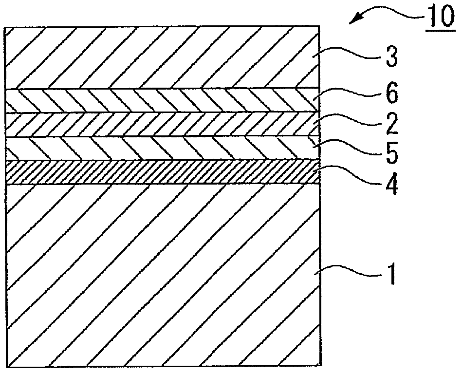
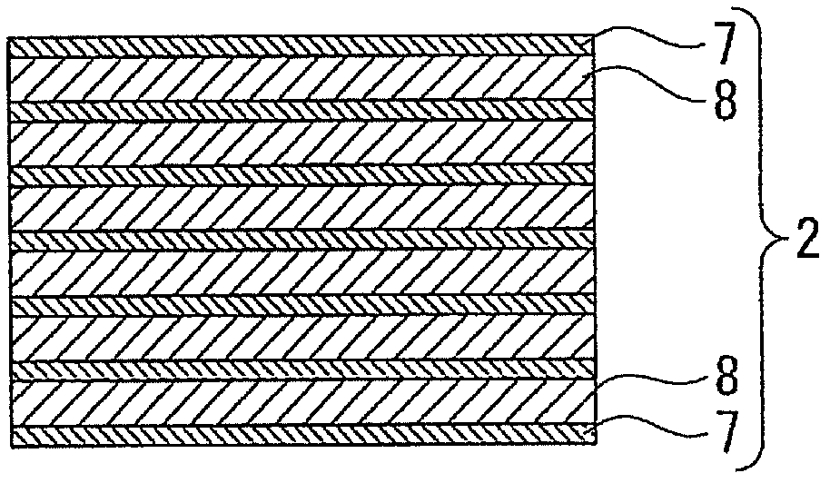
[0105] For the light-emitting diode of Example 1, first, epitaxial growth layers were sequentially stacked on a semiconductor substrate made of Si-doped n-type GaAs single crystal to produce an epitaxial wafer. GaAs substrate, the plane inclined 15° from the (100) plane to the (0-1-1) direction is used as the growth plane, and the carrier concentration is 2×10 18 cm -3 . The so-called epitaxial growth layer is a buffer layer made of Si-doped n-type GaAs, Si-doped n-type (Al 0.5 Ga 0.5 ) 0.5 In 0.5 Low resistance layer composed of P, n-type Al doped with Si 0.5 In 0.5 The lower cladding layer composed of P, undoped Ga 0.44 In 0.56 P / (Al 0.53 Ga 0.47 ) 0.5 In 0.5 Strained light-emitting layer / barrier layer composed of P pairs, p-type Al doped with Mg 0.5 In 0.5 The upper cladding layer composed of P, (Al 0.6 Ga 0.4 ) 0.5 In 0.5 An intermediate layer of a thin film made of P, and a strain adjustment layer made of p-type GaP doped with Mg.
[0106] In this embod...
Embodiment 2
[0116] The light-emitting diode of Example 2 is a light-emitting diode in which only the structures of the strained light-emitting layer and the barrier layer of the light-emitting diode of Example 1 are changed. Here, in the light-emitting diode of Example 2, the strained light-emitting layer of Example 1 above is changed to undoped Ga with a layer thickness of about 10 nm. 0.42 In 0.58 P, change the barrier layer of the above-mentioned embodiment 1 into non-doped (Al 0.53 Ga 0.47 ) 0.5 In 0.5 P, 20 pairs of strained light-emitting layers and barrier layers are stacked alternately.
[0117] Table 1 shows the results of evaluating the characteristics and uniformity of the light-emitting diode lamp equipped with the light-emitting diode of Example 2. As shown in Table 1, when a current was passed between the n-type and p-type ohmic electrodes, red light with a peak wavelength of 660.5 nm was emitted. In addition, the forward voltage (Vf) when a current of 20 milliamps (mA...
Embodiment 3
[0119] The light emitting diode of Example 3 is a light emitting diode in which only the configuration of the strained light emitting layer of the light emitting diode of Example 2 is changed. Here, in the light-emitting diode of Example 3, the strained light-emitting layer of Example 2 above is changed to undoped Ga with a layer thickness of about 15 nm. 0.41 In 0.49 p.
[0120] Table 1 shows the results of evaluating the characteristics and uniformity of the light-emitting diode lamp equipped with the light-emitting diode of Example 3. As shown in Table 1, as a result of flowing current between the n-type and p-type ohmic electrodes, red light with a peak wavelength of 668.0 nm was emitted. In addition, the forward voltage (Vf) when a current of 20 milliamps (mA) flows forward is about 2.0 volts (V). In addition, the light emission output at a forward current of 20 mA was 3.7 mW. The variation in the peak wavelength of all the light-emitting diode lamps assembled was 2.2...
PUM
| Property | Measurement | Unit |
|---|---|---|
| diameter | aaaaa | aaaaa |
| fluorescence wavelength | aaaaa | aaaaa |
| wavelength | aaaaa | aaaaa |
Abstract
Description
Claims
Application Information
 - Generate Ideas
- Intellectual Property
- Life Sciences
- Materials
- Tech Scout
- Unparalleled Data Quality
- Higher Quality Content
- 60% Fewer Hallucinations
Browse by: Latest US Patents, China's latest patents, Technical Efficacy Thesaurus, Application Domain, Technology Topic, Popular Technical Reports.
© 2025 PatSnap. All rights reserved.Legal|Privacy policy|Modern Slavery Act Transparency Statement|Sitemap|About US| Contact US: help@patsnap.com


