Ion source cleaning in semiconductor processing systems
An ion source and ion implantation technology, applied in the field of semiconductor processing systems, can solve problems such as limiting commercial vitality
- Summary
- Abstract
- Description
- Claims
- Application Information
AI Technical Summary
Problems solved by technology
Method used
Image

Examples
example 1
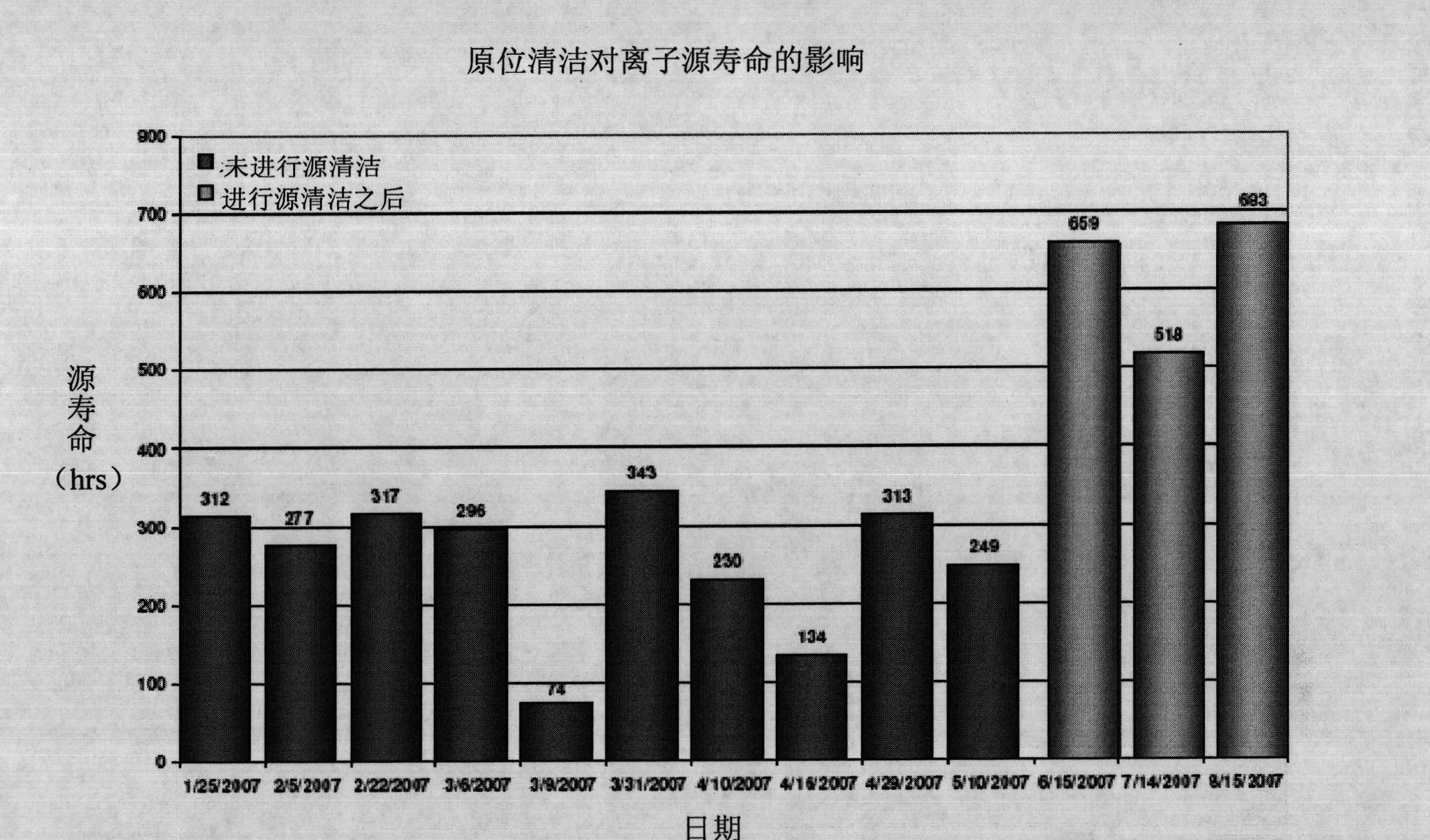
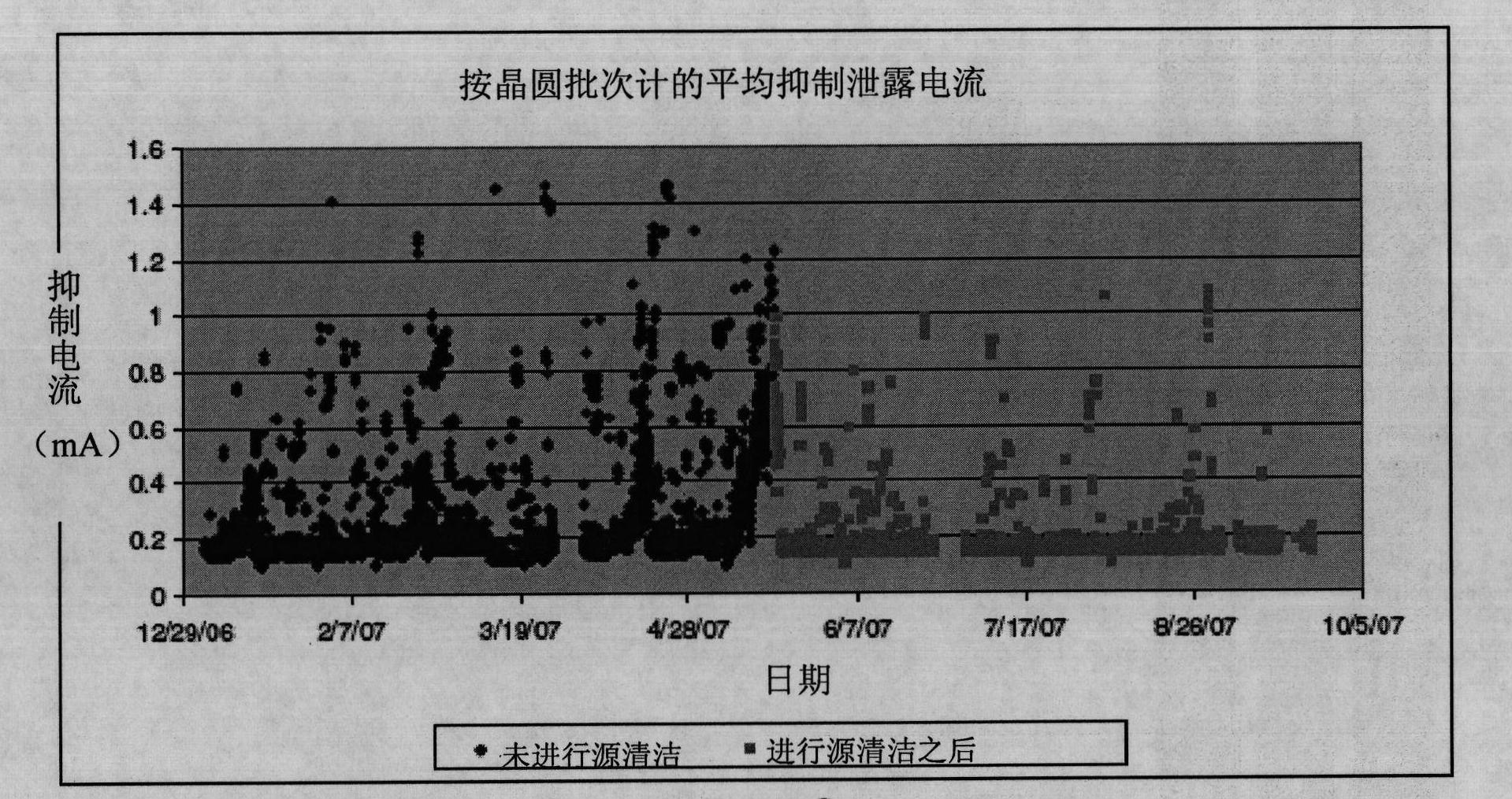
[0170] This example shows improvements in ion source lifetime and implanter utilization that can be achieved by using a chemical cleaner to remove deposits. Preferably, the deposits are removed at regular intervals in order to prevent the accumulation of contaminant flakes and conductive films in the implanter.
[0171] In-situ cleaning is performed at regular intervals from the XeF located in the gas box of the ion implanter. 2 The supply container introduces XeF 2 to carry out, where XeF 2 Purge vapors were introduced into the ion source twice daily for 10-15 minutes each. Experiments were performed using a high current implanter to evaluate the flow kinetics of the cleaning reagent. Identified XeF 2 Cleaning properties and demonstrated that the cleaning agent has no adverse effect on the beam tubing components of the implanter. Therefore, using XeF 2 The reagent cleaning procedure is qualified for use in a moderate current implanter device.
[0172] figure 1 is a gr...
example 2
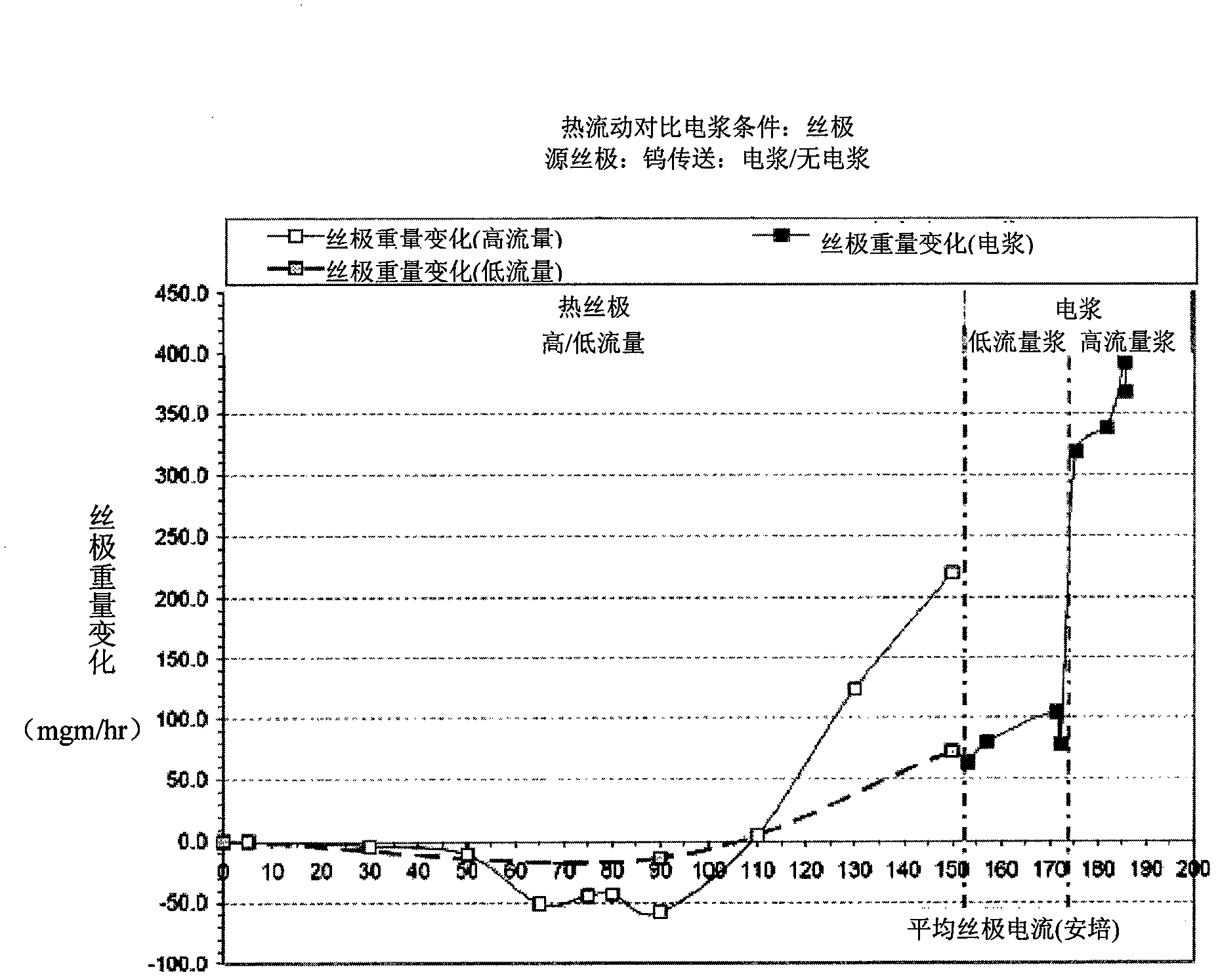
[0187] This example demonstrates the control of filament growth in the ion source of an illustrative ion implanter system.
[0188] Figure 5A shows the XeF in terms of increased filament current and weight 2 A diagram of the effects of current and arc power variations. The figure shows a plot of filament weight (in grams) as a function of elapsed time (in hours) of operation of the implanter system. The upper line in this graph represents XeF at 2.2 standard cubic centimeters per minute (sccm) 2 Flow rate and arc power operation of 100 volts / 0.05 amps, for which a filament weight gain of 319 mg / hour was determined after 3 hours of operation. The lower line in this graph reflects the XeF at 0.5 sccm 2 Flow rate and arc power of 40 volts / 0.05 amps, which produced a filament weight gain of 63 mg / hour over a 3 hour continuous execution time.
[0189] Figure 5B shows the XeF in terms of filament current 2 A diagram of the effect of flow and arc power changes. The figure s...
PUM
 Abstract
Description
Claims
Application Information
 - R&D
- Intellectual Property
- Life Sciences
- Materials
- Tech Scout
- Unparalleled Data Quality
- Higher Quality Content
- 60% Fewer Hallucinations
Browse by: Latest US Patents, China's latest patents, Technical Efficacy Thesaurus, Application Domain, Technology Topic, Popular Technical Reports.
© 2025 PatSnap. All rights reserved.Legal|Privacy policy|Modern Slavery Act Transparency Statement|Sitemap|About US| Contact US: help@patsnap.com