
Preparation method of phosphorescent diode with electronic transmission layer doped with lithium fluoride

A technology of electron transport layer and lithium fluoride, which is applied in the direction of circuits, electrical components, electric solid devices, etc., and can solve the problems of luminous efficiency attenuation and other problems

Inactive Publication Date: 2012-03-28
TAIYUAN UNIV OF TECH
View PDF3 Cites 13 Cited by
  • Summary
  • Abstract
  • Description
  • Claims
  • Application Information

AI Technical Summary

Problems solved by technology

[0002] Organic light-emitting diode (OLED), due to its advantages of high brightness, wide viewing angle, active light emission, low power consumption, and rich light-emitting colors, has a wide range of application prospects in the field of display and lighting. In practical applications, the luminous efficiency and life of OLED are crucial. Important; in organic solid-state luminescence, the excited state of organic molecules is divided into singlet state and triplet state, and the spin statistics calculation shows that the probability of forming singlet state and triplet state excitons is 25% and 75%, so based on the fluorescent material For OLEDs, the upper limit of its internal quantum efficiency is 25%. Compared with OLEDs with traditional fluorescent materials as light-emitting components, organic light-emitting diodes PHOLED with phosphorescent materials can simultaneously utilize singlet and triplet excitons, making the internal quantum efficiency of the device higher. The upper limit reaches 99.99%, so PHOLED has a greater advantage in luminous efficiency; however, one of the biggest problems in phosphorescent devices is the quenching of triplet excitons at high current densities, which leads to a decrease in luminous efficiency at high current densities. Rapid attenuation; the introduction of the double-emitting layer structure makes the light-emitting area of ​​the device no longer concentrated at the interface, but expands to the entire light-emitting layer area, reducing the accumulation of carriers at the interface and reducing the triplet-triplet excitons The annihilation of the device also reduces the degradation of the device caused by charge accumulation, thereby improving the efficiency and life of the device; because the electron transport layer doping can improve the conductivity of the device, reduce the driving voltage of the device, and balance the injection, transport and recombination of carriers , so it can also improve the efficiency and life of the device; Raymond et al. have reported that by changing the hole blocking layer of the device to study the impact of different hole blocking layer materials on OLED performance; found that: using two-(2-methyl-8 -Hydroxyquinoline)-4-(phenylphenol)aluminum as a hole blocking layer, although the device has a long life, under packaging conditions, when the initial brightness is 500cd / m 2 When using 2,2',2"-(1,3,5-benzoyl)-tri-(1-phenyl) -1-H-benzimidazole) replaces bis-(2-methyl-8-hydroxyquinoline)-4-(phenylphenate) aluminum as a hole blocking layer and its efficiency is improved to 25.3cd / A, However, the life of the device is very short. Under packaging conditions, when the initial brightness is 500cd / m 2 The lifetime is only 70h; how to achieve high efficiency and long life of OLED at the same time has always been the goal pursued by OLED research

Method used


Image

  • Preparation method of phosphorescent diode with electronic transmission layer doped with lithium fluoride
  • Preparation method of phosphorescent diode with electronic transmission layer doped with lithium fluoride
  • Preparation method of phosphorescent diode with electronic transmission layer doped with lithium fluoride

Examples


Embodiment Construction

[0123] The present invention will be further described below in conjunction with accompanying drawing:

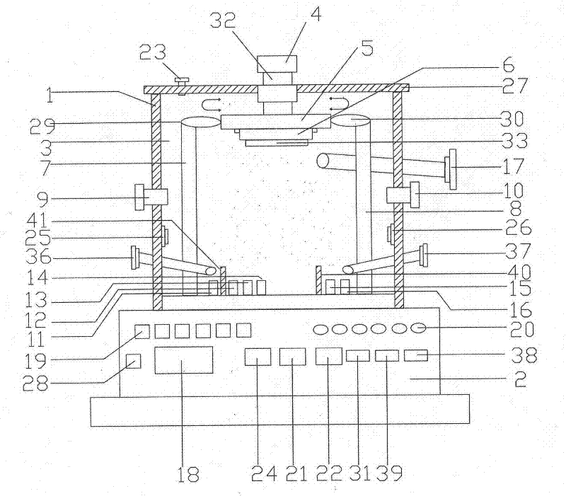
[0124] figure 1 As shown in the figure, the state diagram is prepared for the phosphorescent diode doped with lithium fluoride in the electron transport layer. The position and connection relationship of each part must be correct, according to the ratio of quantity, and operate in sequence.

[0125] The amount of the chemical substance material required for the preparation is determined according to a preset range, with gram, milliliter, millimeter, micron and nanometer as measurement units.

[0126] Evaporation material crucible, put one kind of material in one crucible, do not mix and put, different materials, different heating and sublimation temperature, and adjust the heating and sublimation temperature according to the setting of pressure intensity ≤ 0.0004Pa.

[0127] The preparation of the phosphorescent diode doped with lithium fluoride in the electron transport l...


PUM


Abstract

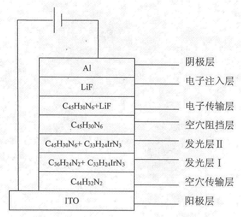
The invention relates to a preparation method of a phosphorescent diode with an electronic transmission layer doped with lithium fluoride. The phosphorescence diode has a eight-layer planar structure that comprises an anode layer, a hole transmission layer, a luminescent layer I, a luminescent layer II, a hole barrier layer, an electronic transmission layer, an electron injection layer and a cathode layer; thris (2-phenylpyridine) iridium is utilized to carry out phosphorescent dye doping on the luminescent layer I and the luminescent layer I so as to form a double luminescent layer; and lithium fluoride is utilized to carry out doping on the electronic transmission layer. The preparation of the phosphorescent diode is carried out in a vacuum vapor plating furnace, wherein the vacuum degree is less than or equal to 0.0004Pa and the temperature in the furnace is from a value by adding 25 DEG C with 2 DEG C to a value by subtracting the 2 DEG C from the 25 DEG C. Processes of heating and sublimation of vapor plating materials, form transformation, vapor deposition and film growth are carried out so as to form a dual-luminescent layer phosphorescent diode with the electronic transmission layer doped with the lithium fluoride, wherein the phosphorescent diode has a thickness of 261.2 nm. Besides, an emission wavelength is 516 nm; a color coordinate is expressed as that x is equal to 0.3151 and y is equal to 0.6054; green lights is emitted; and a maximum value of current efficiency is 39. 03cd / A. Moreover, compared with the prior art, the technology employed in the invention enables luminous efficiency of the diode to be improved by 54%; an initial brightness of a packaging device is 500cd / m <2>; and the device service life is 320h; and the service life of the diode can be improved by 3.57 times.

Description

technical field [0001] The invention relates to a preparation method of a phosphorescent diode whose electron transport layer is doped with lithium fluoride, and belongs to the technical field of design and preparation of organic electroluminescent devices. Background technique [0002] Organic light-emitting diode (OLED), due to its advantages of high brightness, wide viewing angle, active light emission, low power consumption, and rich light-emitting colors, has a wide range of application prospects in the field of display and lighting. In practical applications, the luminous efficiency and life of OLED are crucial. Important; in organic solid-state luminescence, the excited state of organic molecules is divided into singlet state and triplet state, and the spin statistics calculation shows that the probability of forming singlet state and triplet state excitons is 25% and 75%, so based on the fluorescent material For OLEDs, the upper limit of its internal quantum efficien...

Claims


Application Information

Patent Timeline
Patent Type & Authority Applications(China)
IPC IPC(8): H01L51/56
Inventor 郝玉英杨倩房晓红袁树青王振国王华许并社
Owner TAIYUAN UNIV OF TECH
Learn More