
Photonic crystal waveguide terahertz modulator for modulating terahertz waves at high speed

A photonic crystal waveguide and photonic crystal technology, applied in the field of terahertz applications, can solve the problems of low modulation rate, narrow modulation bandwidth and small modulation depth of terahertz modulators, achieve short response time, realize multi-working window intensity modulation and The effect of frequency modulation and wide modulation bandwidth

Inactive Publication Date: 2012-03-28
NANKAI UNIV
View PDF4 Cites 19 Cited by
  • Summary
  • Abstract
  • Description
  • Claims
  • Application Information

AI Technical Summary

Problems solved by technology

[0005] The purpose of the present invention is to provide a photonic crystal waveguide terahertz modulator capable of high-speed modulation of terahertz waves, to solve key technical problems such as narrow modulation bandwidth, low modulation rate, and small modulation depth of the terahertz modulator in the background technology

Method used


Image

  • Photonic crystal waveguide terahertz modulator for modulating terahertz waves at high speed
  • Photonic crystal waveguide terahertz modulator for modulating terahertz waves at high speed
  • Photonic crystal waveguide terahertz modulator for modulating terahertz waves at high speed

Examples


Embodiment Construction

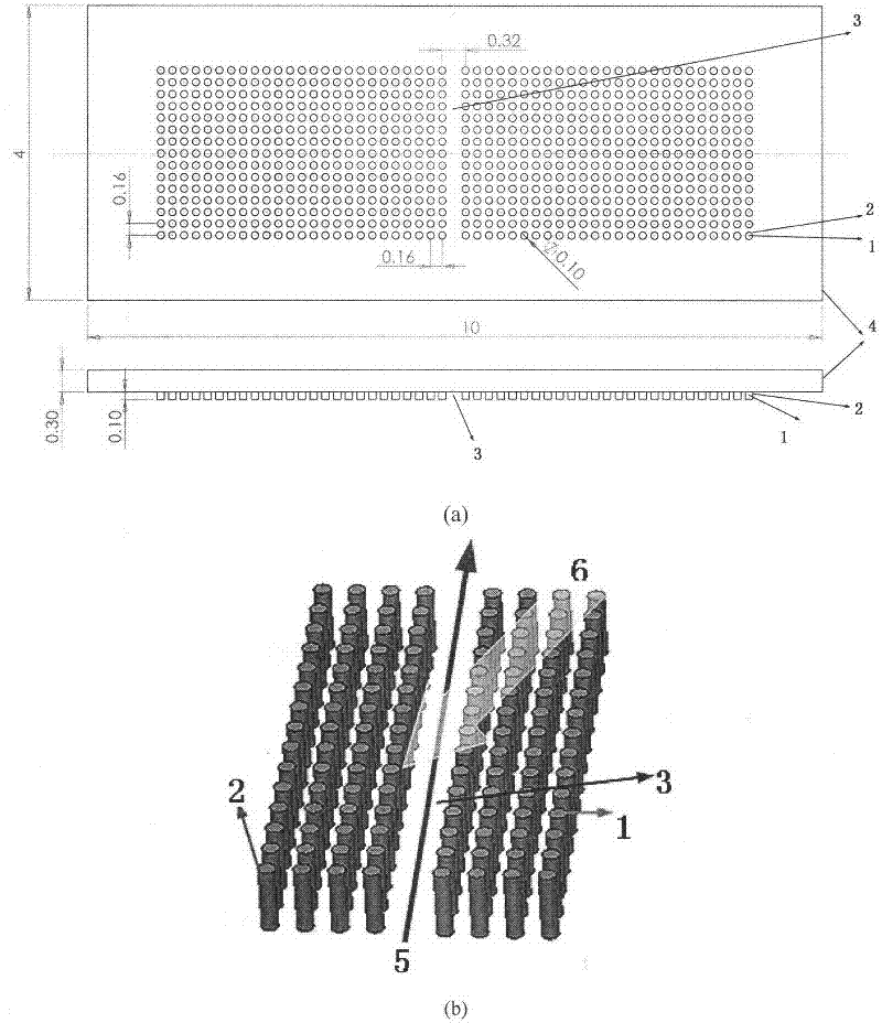
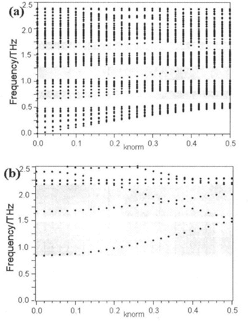
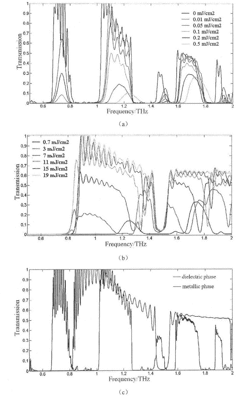
[0020] The working process of the present invention is illustrated by an example of a high-speed photonic crystal waveguide terahertz modulator working around 1THz:

[0021] like figure 1 As shown in (a), the silicon used in the silicon photonic crystal column is high-resistance silicon with a resistance value of 6000 Ω·cm or more. A silicon photonic crystal column array was obtained on a 0.4mm thick double-sided polished high-resistance silicon wafer by MEMS ion beam deep etching process. . A layer of metal vanadium is coated on the processed silicon photonic crystal column by a magnetron sputtering method, and then an oxidation method is used to convert the metal vanadium into a vanadium dioxide film. The conductivity of the vanadium dioxide film in the dielectric phase is less than 0.1 (Ω·cm) -1 , the conductivity in the metallic phase is greater than 2000 (Ω·cm) -1 , with a thickness of 1 μm. like figure 1 As shown in (b), the center wavelength of 800nm ​​Ti:sapphire...


PUM

PropertyMeasurementUnit
Spot diameteraaaaaaaaaa

Abstract

The invention discloses a photonic crystal waveguide terahertz modulator for modulating terahertz waves at high speed. The surface of a silicon photonic crystal pillar array of wired defect waveguide is plated with a layer of vanadium dioxide film, the vanadium dioxide film without laser irradiation at room temperature is a medium phase and the member shows a band gap property of medium photonic crystal waveguide; when the surface of the photonic crystal pile is irradiated by laser, phase change occurs to the vanadium dioxide film and a member shows a bond gap property of metal photonic crystal waveguide. Because the conduction bands of the medium and the metal photonic crystal waveguide of a same structure are completely different, the terahertz strength modulation and frequency modulation of a light-controlled high speed broad bond can be realized. The terahertz modulator modulates the bond width largely, that is, more than 100GHz; the modulation mode is flexible and various and can realize multi-window strength modulation and frequency modulation; the modulation depth is more than 90%; the response time is short and the modulation speed is 100Gbps; and the structure and the modulation method are simple and convenient for minimization and integration, and can meet the requirement on a terahertz communication system.

Description

technical field [0001] The invention belongs to the technical field of terahertz applications, and in particular relates to a high-speed photonic crystal waveguide terahertz modulator and a modulation method thereof. Background technique [0002] Terahertz (THz, 1THz=10 12 THz) wave refers to the electromagnetic wave with frequency in the range of 0.1 ~ 10THz (corresponding wavelength is 3mm ~ 30μm), this band is between microwave and light wave, it is the intersection of electronics and photonics. Due to its special position in the electromagnetic spectrum, terahertz waves have many superior properties such as transparency, safety, and high signal-to-noise ratio, and have very important academic and application values ​​in the fields of spectroscopy, imaging, and communications. Terahertz communication has the advantages of rich frequency band resources, high bandwidth, good confidentiality, anti-electromagnetic interference, and can realize indoor short-distance or space ...

Claims


Application Information

Patent Timeline
IPC IPC(8): G02F1/025
Inventor 范飞常胜江
Owner NANKAI UNIV
Learn More