
Annular-electrode microcavity laser device

A ring electrode and laser technology, applied in lasers, laser parts, semiconductor lasers, etc., can solve problems affecting the modulation speed of lasers and single-mode working performance of microcavity lasers

Inactive Publication Date: 2014-05-21
INST OF SEMICONDUCTORS - CHINESE ACAD OF SCI
View PDF5 Cites 5 Cited by
  • Summary
  • Abstract
  • Description
  • Claims
  • Application Information

AI Technical Summary

Problems solved by technology

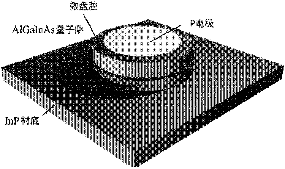
[0006] However, in the process of realizing the present invention, the applicant found that the disk-shaped electrode microcavity laser of the prior art is designed as a disk, and the carriers are mainly distributed in the center of the laser in the active region of the micro-disk laser, while the laser The internal optical field mode is mainly distributed on the edge of the disc-shaped m

Method used


Image

  • Annular-electrode microcavity laser device
  • Annular-electrode microcavity laser device
  • Annular-electrode microcavity laser device

Examples


Embodiment Construction

[0026] In order to make the object, technical solution and advantages of the present invention clearer, the present invention will be described in further detail below in conjunction with specific embodiments and with reference to the accompanying drawings. It should be noted that, in the drawings or descriptions of the specification, similar or identical parts all use the same figure numbers. Implementations not shown or described in the accompanying drawings are forms known to those of ordinary skill in the art. Additionally, while illustrations of parameters including particular values ​​may be provided herein, it should be understood that the parameters need not be exactly equal to the corresponding values, but rather may approximate the corresponding values ​​within acceptable error margins or design constraints. The directional terms mentioned in the embodiments, such as "upper", "lower", "front", "rear", "left", "right", etc., are only referring to the directions of the...


PUM

PropertyMeasurementUnit
Thicknessaaaaaaaaaa

Abstract

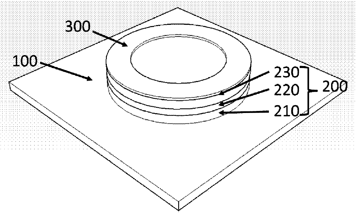
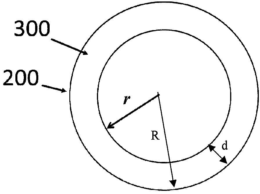
The invention provides an annular-electrode microcavity laser device. The annular-electrode microcavity laser device comprises a substrate, a microcavity laser device formed on the substrate, a first conductive type of patterned electrode made from metal and in an annular shape, and formed at the outer side edge of the top of the microcavity laser device, and a second conductive type of electrode formed on the side surface of the microcavity laser device when the substrate is an insulated substrate, and formed on the back surface of the substrate or the side surface of the microcavity laser device when the substrate is a conductive substrate, wherein the first conductive type and the second conductive type are one of p-type and n-type respectively. According to the annular-electrode microcavity laser device provided by the invention, laser emission mode optical field distribution and carrier distribution are largely superposed in space to acquire a high gain, and then to realize single-mode laser emission.

Description

technical field [0001] The invention relates to the field of semiconductor lasers, in particular to a ring electrode microcavity laser. Background technique [0002] With the advancement and innovation of modern information technology, optoelectronic devices are gradually developing towards high-density integration, high efficiency, low power consumption and miniaturization. [0003] In the on-chip optical interconnection, there are two main methods for converting the loaded electrical signal into an optical signal: one is to convert the light output by the laser through an optical modulator; the other is to convert the electrical signal It is directly loaded on the laser and realized by directly modulating the output optical signal of the laser by the current. At present, the on-chip optical interconnection technology is developing in the direction of low cost, high speed, and low power consumption. [0004] Compared with indirectly modulated microcavity lasers, directly ...

Claims


Application Information

Patent Timeline
IPC IPC(8): H01S5/10H01S5/042
Inventor 吕晓萌邹灵秀龙衡黄永箴
Owner INST OF SEMICONDUCTORS - CHINESE ACAD OF SCI
Learn More