Resin molded article for optical element, method for manufacturing resin molded article for optical element, device for manufacturing resin molded article for optical element, and scanning optical device

A technology for resin molding and optical elements, which is applied in the field of manufacturing equipment for resin molding products for optical elements, and can solve problems such as reducing surface accuracy.

Inactive Publication Date: 2012-02-22
KONICA MINOLTA OPTO
View PDF5 Cites 2 Cited by
  • Summary
  • Abstract
  • Description
  • Claims
  • Application Information

AI Technical Summary

Problems solved by technology

However, there is a time lag in the injection of the gas after filling the resin, so the flow velocity of the tip of the molten resin changes, and sometimes the surface of the tip of the molten resin has abnormal appearance such as stagnation marks due to the stop, and the surface accuracy is significantly reduced.

Method used


Image

  • Resin molded article for optical element, method for manufacturing resin molded article for optical element, device for manufacturing resin molded article for optical element, and scanning optical device
  • Resin molded article for optical element, method for manufacturing resin molded article for optical element, device for manufacturing resin molded article for optical element, and scanning optical device
  • Resin molded article for optical element, method for manufacturing resin molded article for optical element, device for manufacturing resin molded article for optical element, and scanning optical device

Examples


no. 1 Embodiment approach

[0060] structure

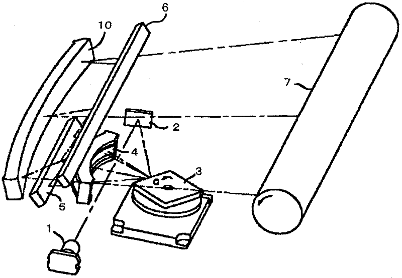
[0061] Reference figure 1 A description will be given of a resin molded product for an optical element according to the first embodiment of the present invention. figure 1 It is a schematic diagram of an example of a laser scanning optical device in which a resin molded product for optical elements is assembled.

[0062] figure 1 Among them, the laser scanning optical device includes a light source unit 1, a cylindrical mirror 2, a polygon mirror 3 as a deflection means, a Toric lens 4, plane mirrors 5 and 6, and an fθ mirror 10 with fθ characteristics.

[0063] The laser light emitted from the light source unit 1 is condensed into a substantially parallel light by a collimator lens (not shown in the figure), and then is reflected by the cylindrical mirror 2, and its beam shape is changed to a substantially linear shape with the longitudinal direction parallel to the main scanning direction , Reach the polygon mirror 3.

[0064] The outer peripheral surface of the ...

no. 2 Embodiment approach

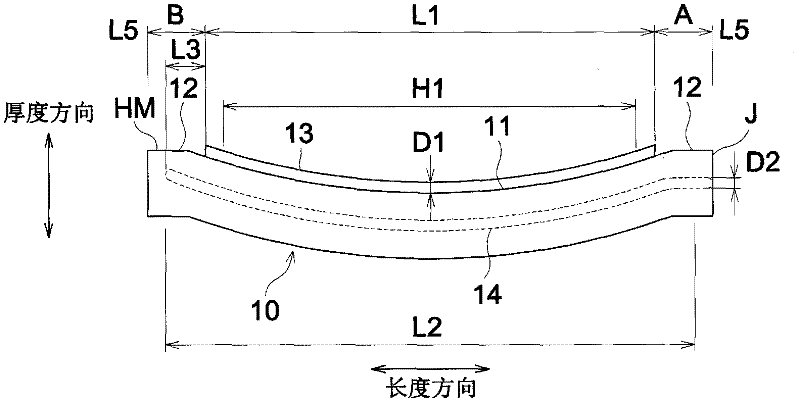
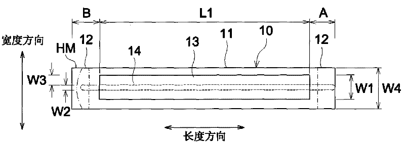
[0146] Next reference Figure 13 , Figure 14 A description will be given of the resin molded product for an optical element according to the second embodiment of the present invention. Figure 13 It is a plan view of a resin molded product for optical components, Figure 14 This is a cross-sectional view of a resin molded product for optical elements. Regarding the resin molded product for optical elements of the first embodiment described above, the fθ mirror 10 is representatively described, and the resin molded product for optical elements of the second embodiment is representatively described fθ lens 20.

[0147] The fθ lens 20 is provided in the laser scanning optical device like the fθ mirror 10. The fθ mirror 10 has a mirror surface 13 that reflects laser light, while the fθ lens 20 has an optical surface 23 that transmits laser light. The fθ lens 20 having the optical surface 23 also has the same function as the fθ mirror 10, and converts the speed of laser light deflect...

Embodiment

[0168] Hereinafter, the present invention will be explained based on preferred embodiments. The resin molded product manufactured in the example is the base material of the fθ mirror 10. The comparative example is also the base material of the fθ mirror 10.

[0169] Using the above manufacturing device and manufacturing method, the cavity shape is image 3 The type shown is molded and manufactured with the following two types of molds.

[0170] Type 1

[0171] A=B=5.0mm

[0172] Of the two fθ mirrors obtained by evaluation and molding, both of them confirmed that the shape deterioration caused by sinking or the like on the entire first surface portion was suppressed, and a mirror shape with high surface accuracy was obtained.

[0173] In addition, by using this mirror in a scanning optical device using laser light with a wavelength of 408 nm, it was confirmed that the spots were highly concentrated and high-definition image formation was possible.

[0174] Type 2

[0175] As a compar...


PUM

PropertyMeasurementUnit
surface roughnessaaaaaaaaaa

Abstract

Provided is: a resin molded article for an optical element wherein high surface precision is kept since an abnormal appearance-formed portion such as a hesitation mark is effectively formed outside an optical surface without cutting off the portion and an optical surface itself can be less likely to be influenced by shrinkage with hardening such as sink; a method and device for manufacturing the same; and a scanning optical device. The resin molded article for an optical element which comprises first surface portion at a part of the surface of a resin molded base and comprises a hollow portion formed by injecting a fluid into the inside of the base from the outside. Assuming that the distance between the first end of the base and an end of the first surface portion, the end being close to the first end, is A and the distance between the second end of the base, the end being other than the first end and being on the opposite side across the first surface portion, and the end of the first surface portion, the end being on the side close to the second end, is B, the relations of (A>0, B>0, A=B) are satisfied.

Description

Technical field [0001] The present invention relates to a resin molded product for an optical element, a method for manufacturing a resin molded product for an optical element, an apparatus for manufacturing a resin molded product for an optical element, and a scanning optical device, and more particularly to a resin filled in a mold cavity by injecting a fluid A resin molded product for an optical element in which a hollow portion is formed, a method for manufacturing a resin molded product for an optical element, an apparatus for manufacturing a resin molded product for an optical element, and a scanning optical device. Background technique [0002] As such optical elements, glass, metal, or ceramics are generally known. In recent years, resins have begun to be used for ease of molding, design freedom, or cost reduction. [0003] Such optical elements are used in various applications. As an example, there are known devices that condense light emitted from a light source to form a...

Claims


Application Information

Patent Timeline
Patent Type & Authority Applications(China)
IPC IPC(8): B29C45/00B29C45/26B29C45/77
CPCB29C45/0025B29C45/1704B29C45/7613B29C2945/7604B29C2945/76167B29C2945/76257B29C2945/76397B29C2945/76454B29C2945/76474B29C2945/76488B29C2945/76585B29C2945/76943B29L2011/0058Y10T428/1352B29C45/00B29C45/26B29C45/77
Inventor 原新一朗真岛利行松本安弘
Owner KONICA MINOLTA OPTO
Why Eureka
Try Eureka