Optical recording medium
A technology for optical recording media and recording layers, applied to optical recording media, optical recording/reproduction, data recording, etc., to achieve high storage reliability, maintain productivity, and high productivity
- Summary
- Abstract
- Description
- Claims
- Application Information
AI Technical Summary
Problems solved by technology
Method used
Image
Examples
Embodiment
[0099] The present invention is specifically described below by means of specific examples, but the present invention is not limited to these examples.
[0100] (method of analyzing layer composition)
[0101] In Examples, Comparative Examples and Test Examples, the composition of each layer was determined as described below.
[0102] First, a layer whose composition is to be determined (for example, a first protective layer or a second protective layer) is deposited on a flat substrate under the same conditions as described in Examples, Comparative Examples, and Test Examples. Thus, samples were prepared. Next, the layer composition of each sample was examined using ICP mass spectrometry using an inductively coupled plasma (ICP) mass spectrometer.
[0103] (Measurement of average thickness)
[0104] In Examples, Comparative Examples and Test Examples, the average thickness of each layer was determined as described below.
[0105]First, a layer whose thickness is to be mea...
Embodiment 1
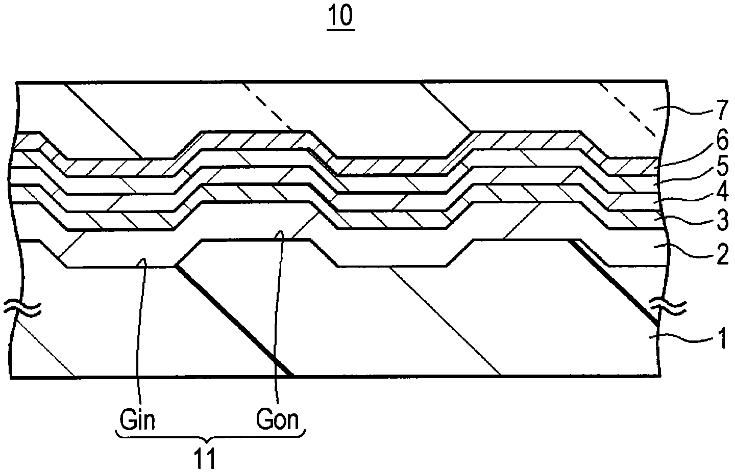
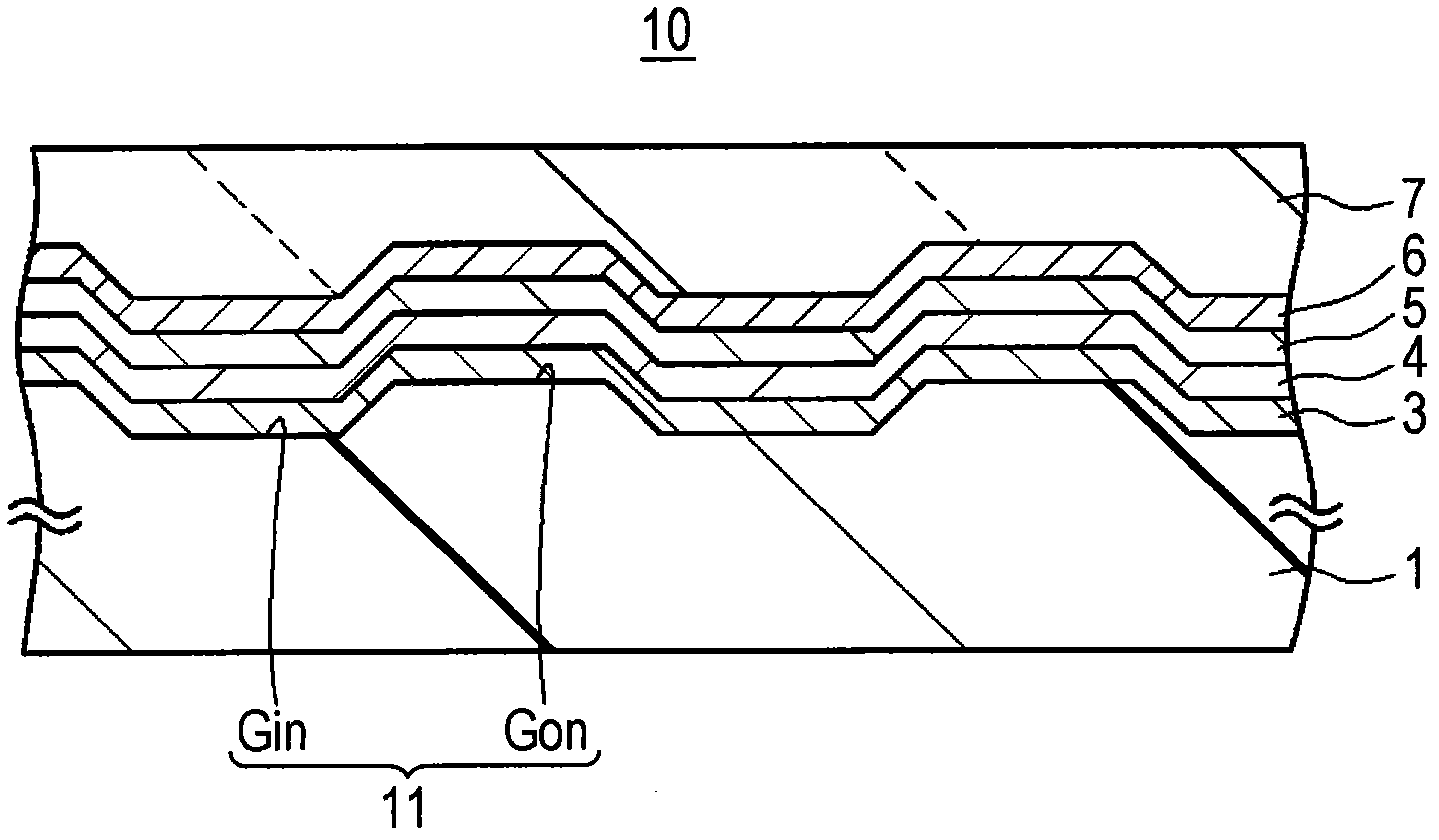
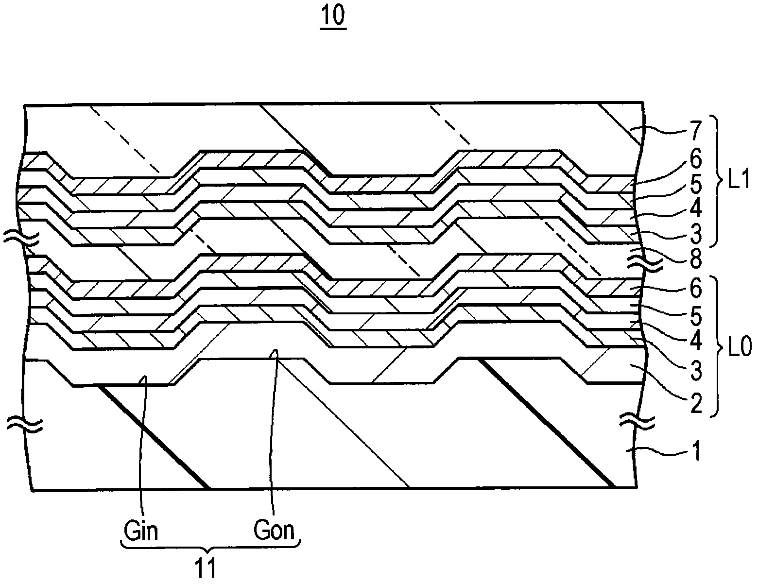
[0175] First, a polycarbonate substrate with a thickness of 1.1 mm was formed by injection molding. An uneven surface with grooves is formed on a polycarbonate substrate. Next, a third protective layer, an inorganic recording layer, a first protective layer, and a second protective layer were sequentially stacked on the polycarbonate substrate by a sputtering method. The specific structure of each layer is as follows.
[0176] The third protective layer: ITO, 8nm (average thickness)
[0177] Inorganic recording layer: [(ZnS) 80 (SiO 2 ) 20 ] 40 Sb 60 , 11nm (average thickness)
[0178] The first protective layer: ITO, 19nm (average thickness)
[0179] Second protective layer: TiO 2 , 10nm (average thickness)
[0180] Each layer was formed using a target with a diameter of 200 mm. The ITO layer used as the first protective layer and the third protective layer is passed through containing Ar and O 2 Deposited by DC sputtering of an ITO target in an atmosphere of . [...
Embodiment 2
[0183] A write-once optical recording medium was prepared according to the method of Example 1, except that the second protective layer was formed of a composite oxide of zirconia, indium oxide, and silicon oxide (SIZ).
PUM
| Property | Measurement | Unit |
|---|---|---|
| thickness | aaaaa | aaaaa |
| thickness | aaaaa | aaaaa |
| wavelength | aaaaa | aaaaa |
Abstract
Description
Claims
Application Information
 - R&D Engineer
- R&D Manager
- IP Professional
- Industry Leading Data Capabilities
- Powerful AI technology
- Patent DNA Extraction
Browse by: Latest US Patents, China's latest patents, Technical Efficacy Thesaurus, Application Domain, Technology Topic, Popular Technical Reports.
© 2024 PatSnap. All rights reserved.Legal|Privacy policy|Modern Slavery Act Transparency Statement|Sitemap|About US| Contact US: help@patsnap.com


