Composite substrate, preparation method of composite substrate and method for preparing single crystal thick film through hetero-epitaxy

A composite substrate and a manufacturing method technology, applied in the directions of single crystal growth, single crystal growth, chemical instruments and methods, etc., can solve problems such as unfavorable industrialization, cracking of sapphire substrates, gallium nitride single crystal thick films and sapphire substrates Problems such as warping of the overall structure

Inactive Publication Date: 2012-01-04
青岛铝镓光电半导体有限公司
View PDF5 Cites 9 Cited by
  • Summary
  • Abstract
  • Description
  • Claims
  • Application Information

AI Technical Summary

Problems solved by technology

[0005] However, since the thermal expansion coefficient of sapphire is greater than that of gallium nitride, when cooling from the growth temperature to room temperature, the lattice change of sapphire is greater than that of gallium nitride, so that tensile stress will be generated on the sapphire substrate , compressive stress is generated on the GaN single crystal thick film, and the overall structure of the GaN single crystal thick film and the sapphire substrate will warp after cooling down to room temperature
At present, the thickness of the sapphire substrate of the general industrial specification is 430 microns. If the thickness of the grown gallium nitride single crystal thick film reaches a certain value (such as exceeding 200 microns), the tensile stress on the sapphire substrate will reach more than 200 MPa. , and the thickness of the grown gallium nitride single crystal usually reaches more than 400 microns, when the tensile stress generated on the sapphire exceeds its fracture stress, it will cause the sapphire substrate to crack
[0006] When the sapphire substrate is broken, the following two factors will also lead to cracking of the gallium nitride single crystal: first, the interface between sapphire and gallium nitride is continuous, and the gallium nitride on the sapphire is broken at the moment of cracking. Cracking of single crystal thick film; Second, cracking of gallium nitride single crystal thick film due to warping deformation
Based on this, the size of the GaN single crystal thick film obtained is often smaller than the size of the original sapphire substrate, which limits the size of the GaN single crystal thick film grown by the HVPE method, which is not conducive to the industrialization of this method.

Method used


Image

  • Composite substrate, preparation method of composite substrate and method for preparing single crystal thick film through hetero-epitaxy
  • Composite substrate, preparation method of composite substrate and method for preparing single crystal thick film through hetero-epitaxy
  • Composite substrate, preparation method of composite substrate and method for preparing single crystal thick film through hetero-epitaxy

Examples


Embodiment 1

[0038] In this example, refer to figure 1 As shown, the composite substrate 200 includes a foreign substrate 100 and a buffer layer 110 on the foreign substrate 100, and the thickness of the foreign substrate 100 is 0.5-13 millimeters.

[0039] More preferably, the thickness of the foreign substrate 100 is 3-8 mm.

[0040] In the present invention, heterogeneous substrate refers to non-nitride substrates such as sapphire, silicon carbide, single crystal silicon, zinc oxide, etc., and the buffer layer is a nitride film, such as aluminum nitride, gallium nitride or gallium nitride alloy, etc. , the thickness of the buffer layer may be less than 50 microns, more preferably, less than 10 microns.

[0041] In the present invention, the composite substrate is used for the epitaxial growth of a group III nitride semiconductor single crystal thick film, such as gallium nitride, aluminum nitride, indium nitride and the like.

[0042] In the composite substrate 200 in this embodiment,...

Embodiment 2

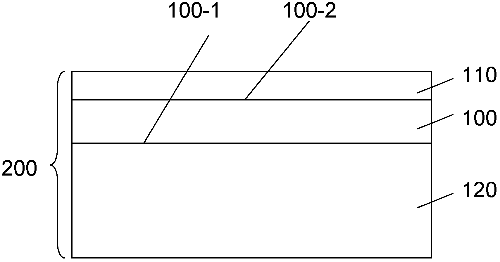
[0050] In this example, refer to figure 2 As shown, the composite substrate 200 includes: a first substrate 120, a foreign substrate 100 on the first substrate 120, and a buffer layer 110 on the foreign substrate 100, wherein the first substrate 120 and the foreign substrate 120 are The heterogeneous substrate 100 has the same thermal expansion coefficient, or the thermal expansion coefficient difference between the first substrate 120 and the heterogeneous substrate 100 is less than 60%, and the thickness of the first substrate 120 is 0.5 to 13 mm.

[0051] More preferably, the first base 120 has a thickness of 3 to 8 mm.

[0052] In this embodiment, the first base 120 and the foreign substrate 100 may have the same coefficient of thermal expansion, that is, the first base and the foreign substrate are made of the same substrate material, for example, the foreign Both the solid substrate and the first base are sapphire, silicon carbide, single crystal silicon or zinc oxide....


PUM

PropertyMeasurementUnit
thicknessaaaaaaaaaa
thicknessaaaaaaaaaa
thicknessaaaaaaaaaa

Abstract

The embodiment of the invention discloses a composite substrate which is used to prepare a nitride (III) semiconductor single crystal thick film through epitaxial growth. The composite substrate is characterized by comprising a heterogeneous substrate and a buffer layer on the heterogeneous substrate, wherein the thickness of the heterogeneous substrate is 0.5-13mm. As the composite substrate has high thickness, after the single crystal thick film is grown on the composite substrate and the growing temperature is reduced to the room temperature, the stress on the composite substrate is less than the fracture stress; and when the single crystal thick film has proper or even higher thickness, the composite substrate can not be broken and then the single crystal thick film can not be broken. Therefore, the size of the formed single crystal thick film can be ensured and the large crystal thick film can be obtained.

Description

technical field [0001] The invention relates to semiconductor manufacturing technology, more specifically, to a composite substrate and a manufacturing method thereof, and a method for preparing a single crystal thick film by heteroepitaxial growth. Background technique [0002] The third-generation semiconductor materials are also called wide-bandgap semiconductors because their energy bandgap is generally greater than 3.0 electron volts. Compared with traditional silicon-based and gallium arsenide-based semiconductor materials, wide bandgap semiconductors, such as silicon carbide (SiC), gallium nitride (GaN), aluminum nitride (AlN) and indium nitride (InN), etc., due to Its unique band gap range, excellent optical and electrical properties and excellent material properties can meet the working requirements of high-power, high-temperature, high-frequency and high-speed semiconductor devices. Wide application prospects. Among them, gallium nitride, aluminum nitride and ind...

Claims


Application Information

Patent Timeline
Patent Type & Authority Applications(China)
IPC IPC(8): C30B25/18C30B29/38H01L29/06H01L21/02
Inventor 刘良宏庄德津
Owner 青岛铝镓光电半导体有限公司
Why Eureka
Try Eureka