Manufacturing method and structure of high-voltage direct-current light-emitting diode chip

A light-emitting diode, high-voltage DC technology, applied in electrical components, electrical solid-state devices, circuits, etc., can solve the problems of device reliability, service life luminous performance, increase peripheral circuits, and peripheral circuit design difficulties, etc., to achieve good products. efficiency and productivity, reducing drive current, and improving internal thermal characteristics

Inactive Publication Date: 2011-11-23
EPILIGHT TECH
View PDF5 Cites 6 Cited by
  • Summary
  • Abstract
  • Description
  • Claims
  • Application Information

AI Technical Summary

Problems solved by technology

However, for low-power light-emitting diodes used in semiconductor lighting, if a 40-watt semiconductor lamp is to be made, more single independent tube cores need to be connected in series; due to the large number of tubes used, more complex peripheral circuits and drivers need to be added
This not only brings difficulty to the design of the peripheral circuit, but also the complex circuit structure will also have a negative impact on the reliability, service life and luminous performance of the device.

Method used


Image

  • Manufacturing method and structure of high-voltage direct-current light-emitting diode chip
  • Manufacturing method and structure of high-voltage direct-current light-emitting diode chip
  • Manufacturing method and structure of high-voltage direct-current light-emitting diode chip

Examples


Embodiment Construction

[0030] The specific implementation steps of the present invention will be further described below in conjunction with the accompanying drawings. For the convenience of illustration, the accompanying drawings are not drawn to scale.

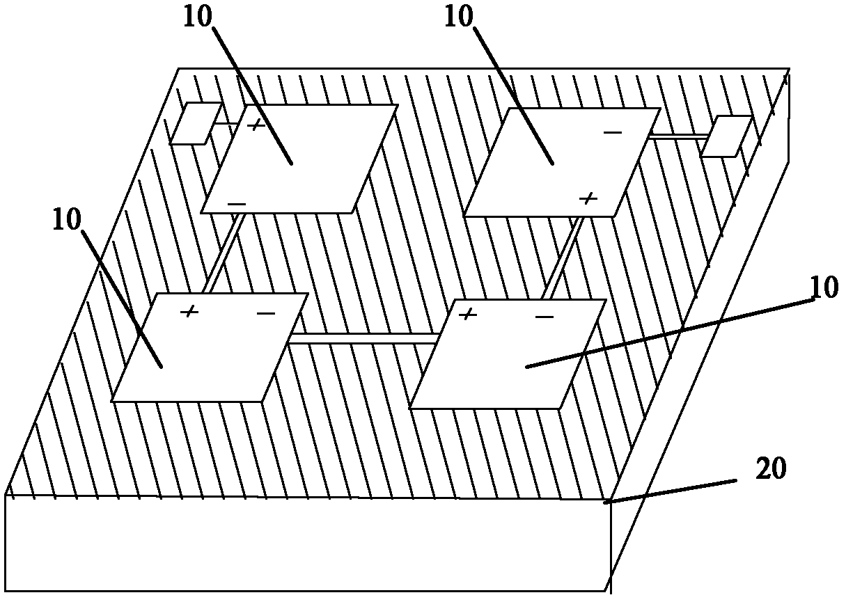
[0031] The high-voltage DC light-emitting diode chip structure provided by the present invention, such as figure 1 As shown, it includes: a plurality of LED (light emitting diode) chip units 10 and a chip substrate 20; each LED chip unit 10 at least sequentially includes an N-type semiconductor layer, an active layer and a P-type semiconductor layer, and is connected with the N-type semiconductor layer respectively. An N electrode and a P electrode electrically connected to the P-type semiconductor layer, the N electrode and the P electrode are located on the same surface of the LED chip unit 10; as figure 2 As shown, the chip substrate 20 includes a thermally conductive substrate 21, an insulating layer 22 located on the thermally conductive sub...


PUM


Abstract

The invention discloses a manufacturing method and a structure of a high-voltage direct-current light-emitting diode chip. The manufacturing method comprises the following steps of: flipping a plurality of selected light-emitting diode chip units on the surface of a high-thermal-conductivity substrate provided with a serial circuit with a flipping process and bonding chips flipped on the substrate with bonding equipment to connect the plurality of light-emitting diode chip units in series in sequence; performing laser stripping on the chips connected in series to a heat conducting substrate and removing a sapphire substrate; and forming a high-voltage direct-current light-emitting diode. In the method, the conventional chip unit is bonded on the high-thermal-conductivity chip substrate provided with the serial circuit for sapphire stripping; the method is simple, is easy to operate and contributes to increasing the chip yield and the production efficiency; and in a manufactured chip structure, the input power of chips can be increased by increasing serial chips, so that the heat injury of a pn junction in a large-current working state is reduced, and the reduction in the luminous efficiency, caused by over high density of current flowing through the pn junction, is prevented. Meanwhile, the high-thermal-conductivity substrate and relatively small working current are adopted, so that heat damage to the chips is reduced, and the service life of the chips is further prolonged.

Description

technical field [0001] The invention relates to a method for manufacturing a light-emitting diode chip and its structure, in particular to a method for manufacturing a high-voltage direct current light-emitting diode chip used in the field of semiconductor lighting and its structure. Background technique [0002] Light-emitting diodes have the advantages of small size, high efficiency and long life, and are widely used in traffic indication, outdoor full-color display and other fields. In particular, the use of high-power light-emitting diodes may realize semiconductor solid-state lighting, which has caused a revolution in the history of human lighting, and has gradually become a research hotspot in the field of electronics. [0003] The traditional chip manufacturing process is to prepare hundreds or even thousands of chips on a substrate at the same time. There is a certain distance between each chip. After these chips are prepared, they are separated by dicing and cutting...

Claims


Application Information

Patent Timeline
Patent Type & Authority Applications(China)
IPC IPC(8): H01L33/00H01L25/075H01L33/48H01L33/62
Inventor 张楠朱广敏李睿郝茂盛
Owner EPILIGHT TECH
Why Eureka
Try Eureka