Preparation method of non-volatile charge storage device, non-volatile charge storage device and application of device
A charge storage and device technology, applied in the field of microelectronic materials, can solve the problems of unbearable device leakage current, inability to function as an insulating medium, and poor data retention performance
- Summary
- Abstract
- Description
- Claims
- Application Information
AI Technical Summary
Problems solved by technology
Method used
Image


Examples
Embodiment 1
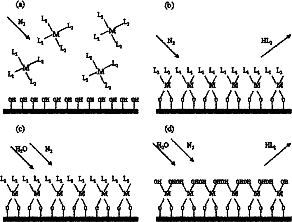
[0033] Embodiment 1: based on p-Si substrate, Si / Al 2 o 3 / (HfO 2 ) 0.8 (Al 2 o 3 ) 0.2 / Al 2 o 3 / Pt charge storage device preparation process is as follows:
[0034] (a) Put the p-Si substrate into an appropriate amount of acetone. After ultrasonic cleaning, use deionized water to ultrasonically clean the substrate to rinse off the residual impurities on the substrate surface. Then the substrate is soaked in hydrofluoric acid to remove surface oxides, then ultrasonically cleaned with deionized water, dried with high-purity nitrogen, and then placed in an atomic layer chemical vapor deposition chamber for thin film deposition.
[0035] (b) HfCl is used in the deposition process 4 and Al(CH 3 ) 3 As a metal source, water is a source of oxygen. Al(CH 3 ) 3 With the nitrogen gas entering the cavity, it reacts with the surface of the hydroxyl-terminated silicon substrate and reaches saturation, and then the oxygen source is brought into the cavity by the nitrogen ga...
Embodiment 1
[0041] Comparative example 1: based on p-Si substrate, Si / Al 2 o 3 / HfO 2 / Al 2 o 3 / Pt charge storage device preparation process is as follows:
[0042] (a) Put the p-Si substrate into an appropriate amount of acetone. After ultrasonic cleaning, use deionized water to ultrasonically clean the substrate to rinse off the residual impurities on the substrate surface. Then the substrate is soaked in hydrofluoric acid to remove surface oxides, then ultrasonically cleaned with deionized water, dried with high-purity nitrogen, and then placed in an atomic layer chemical vapor deposition chamber for thin film deposition.
[0043] (b) HfCl is used in the deposition process 4 and Al(CH 3 ) 3 As a metal source, water is a source of oxygen. Al(CH 3 ) 3 With the nitrogen gas entering the cavity, it reacts with the surface of the hydroxyl-terminated silicon substrate and reaches saturation, and then the oxygen source is brought into the cavity by the nitrogen gas to react with th...
Embodiment 2
[0049] Example 2: Si / Al with different tunneling layer thicknesses based on p-Si substrate 2 o 3 / (HfO 2 ) 0.8 (Al 2 o 3 ) 0.2 / Al 2 o 3 / Pt charge storage device preparation process is as follows:
[0050] (a) Put the p-Si substrate into an appropriate amount of acetone. After ultrasonic cleaning, use deionized water to ultrasonically clean the substrate to rinse off the residual impurities on the substrate surface. Then the substrate is soaked in hydrofluoric acid to remove surface oxides, then ultrasonically cleaned with deionized water, dried with high-purity nitrogen, and then placed in an atomic layer chemical vapor deposition chamber for thin film deposition.
[0051] (b) HfCl is used in the deposition process 4 and Al(CH 3 ) 3 As a metal source, water is a source of oxygen. Al(CH 3 ) 3 With the nitrogen gas entering the cavity, it reacts with the surface of the hydroxyl-terminated silicon substrate and reaches saturation, and then the oxygen source is bro...
PUM
 Abstract
Description
Claims
Application Information
 - R&D
- Intellectual Property
- Life Sciences
- Materials
- Tech Scout
- Unparalleled Data Quality
- Higher Quality Content
- 60% Fewer Hallucinations
Browse by: Latest US Patents, China's latest patents, Technical Efficacy Thesaurus, Application Domain, Technology Topic, Popular Technical Reports.
© 2025 PatSnap. All rights reserved.Legal|Privacy policy|Modern Slavery Act Transparency Statement|Sitemap|About US| Contact US: help@patsnap.com