Chip and preparation method thereof

A chip and oxide technology, applied in the field of storage, can solve the problem of bypass current problem, etc., to avoid misreading phenomenon, increase capacity, and solve the effect of bypass current

Inactive Publication Date: 2011-10-05
SUN YAT SEN UNIV
View PDF5 Cites 1 Cited by
  • Summary
  • Abstract
  • Description
  • Claims
  • Application Information

AI Technical Summary

Problems solved by technology

However, there are still few ways to solve the bypass current problem of bipolar resistive switching devices (resistive switching devices whose resistance change is controlled by the voltage direction)

Method used


Image

  • Chip and preparation method thereof
  • Chip and preparation method thereof
  • Chip and preparation method thereof

Examples


Embodiment Construction

[0037] The present invention will be further described below in conjunction with the accompanying drawings and specific embodiments.

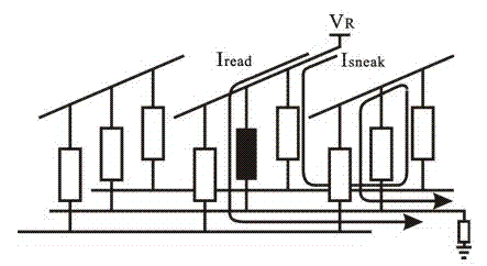
[0038] The chip of this embodiment includes a basic memory unit, the basic memory unit is a resistive memory device, the resistive memory device includes a conductive doped oxide substrate, and the opposite of the doped oxide substrate Metal electrodes made of the first metal material and the second metal material are respectively provided on both sides to form a structure of the first metal electrode / doped oxide substrate / second metal electrode, such as figure 2 shown. Wherein the first metal electrode and the second metal electrode form a contact barrier with the doped oxide substrate. That is, the work function of the first metal material and the second metal material must be greater than the work function of the doped oxide used, so that a contact barrier can be formed. The above-mentioned memory device is different from other devices in...


PUM

PropertyMeasurementUnit
thicknessaaaaaaaaaa
diameteraaaaaaaaaa

Abstract

The invention belongs to the technical field of storage and provides a chip which comprises a basic storage unit, wherein the basic storage unit is a resistance-variable storage device which comprises a conductive doped oxide substrate; a metal electrode made of a first metal material and a second metal material is respectively arranged at two opposite sides of the doped oxide substrate to form a first metal electrode / doped oxide substrate / second metal electrode structure; and the first metal electrode and the second metal electrode form a contact barrier with the doped oxide substrate. The invention further provides a preparation method of the chip. The capacity of the chip provided by the invention is greatly improved while the write-in current of the device is reduced, thereby reducing the chip consumption.

Description

technical field [0001] The invention belongs to the technical field of storage, and in particular relates to a chip for high-density non-volatile storage and a preparation method thereof. Background technique [0002] In recent years, people have been pursuing a general-purpose information storage technology. This technology should combine the non-volatility of flash memory (that is, the characteristics of data retention after power failure) and the high-speed read and write characteristics of memory. power consumption, which can realize the characteristics of high-density storage. Resistive switching device is a new type of memory device based on nano-ion effect. In such devices, ions in the material migrate under the action of an electric field, changing the device resistance. To put it simply, there are two ways in which ion movement can change the resistance of a device. One is that the ion migration forms a conductive channel in the insulating material, and the break ...

Claims


Application Information

Patent Timeline
Patent Type & Authority Applications(China)
IPC IPC(8): H01L27/115H01L21/8247
Inventor 杨眉李树玮
Owner SUN YAT SEN UNIV
Why Eureka
Try Eureka