One-phase ferroelectric film and preparing method thereof as well as effective resistance regulation mode
A technology of ferroelectric thin film and effective resistance, which is applied in the field of microelectronic materials, can solve the problems of not considering the modulation effect of effective resistance, introduce ferroelectric performance and semiconductor performance at the same time, achieve short polarization time, improve fatigue resistance performance, and extremely small area effect
- Summary
- Abstract
- Description
- Claims
- Application Information
AI Technical Summary
Problems solved by technology
Method used
Image
Examples
Embodiment 1
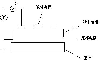
[0031] On Pt / TiO 2 / Ti / SiO 2 / Si substrates grow BiFeO 3 (200 nm) and Bi 0.85 Nd 0.15 FeO 3 (200 nm) thin film, as attached figure 1 shown.
[0032] (1) The epitaxial ferroelectric film was grown by magnetron sputtering method, and Pt was used as the top and bottom electrodes, and the Pt / TiO 2 / Ti / SiO 2 / Si substrates grow BiFeO 3 (200 nm) and Bi 0.85 Nd 0.15 FeO 3 (200 nm) films, followed by BiFeO 3 and Bi 0.85 Nd 0.15 FeO 3 The Pt top electrode is grown on the thin film.
[0033] (2) The specific growth conditions are: control Pt / TiO 2 / Ti / SiO 2 / Si substrate temperature is 400°C, in O 2 The pressure in the atmosphere is 1Pa, the sputtering power is 500W, and annealing is performed at 400°C for 30 minutes after the deposition is completed.
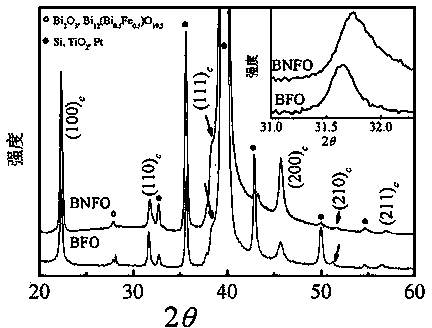
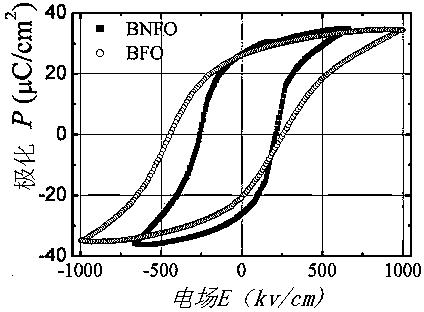
[0034] (3) Using XRD diffraction and ferroelectric tester to test the prepared BiFeO 3 (200nm) / Pt / TiO 2 / Ti / SiO 2 / Si film and Bi 0.85 Nd 0.15 FeO 3 (200nm) / Pt / TiO 2 / Ti / SiO 2 / Si thin film was analyzed, and th...
Embodiment 2
[0039] By Bi 0.8 Ca 0.1 FeO 3-d (100 nm) / SrRuO 3 (50 nm) / (001) c SrTiO 3 Thin film as an example:
[0040] (1) Preparation of Bi 0.8 Ca 0.1 FeO 3-d and SrRuO 3 target, where SrRuO 3 (50 nm) as top and bottom electrodes (100) c SrTiO 3 as a substrate.
[0041] (2) The film was prepared by pulsed laser deposition method, using (001) c SrTiO 3 As a substrate, SrRuO 3 (50 nm) as the top and bottom electrodes, grow epitaxial ferroelectric films, first at (100) c SrTiO 3 SrRuO grown on substrate 3 (50 nm) bottom electrode thickness, followed by SrRuO 3 (50 nm) / (100) c SrTiO 3 Growth Bi 0.8 Ca 0.1 FeO 3-d The film thickness is 100 nm, and finally again in Bi 0.8 Ca 0.1 FeO 3-d Growth of SrRuO on Thin Films 3(50 nm) as the top electrode.
[0042] (3) Specific growth method: install the substrate and the target in the growth chamber, and then use a mechanical pump and a molecular pump to evacuate it. Before deposition, the substrate temperatur...
PUM
| Property | Measurement | Unit |
|---|---|---|
| thickness | aaaaa | aaaaa |
Abstract
Description
Claims
Application Information
 - R&D
- Intellectual Property
- Life Sciences
- Materials
- Tech Scout
- Unparalleled Data Quality
- Higher Quality Content
- 60% Fewer Hallucinations
Browse by: Latest US Patents, China's latest patents, Technical Efficacy Thesaurus, Application Domain, Technology Topic, Popular Technical Reports.
© 2025 PatSnap. All rights reserved.Legal|Privacy policy|Modern Slavery Act Transparency Statement|Sitemap|About US| Contact US: help@patsnap.com


