TSV (through silicon via) chip bonding structure

A chip bonding and bonding structure technology, applied in the field of microelectronics, can solve the problem of not being a solution, and achieve the effect of preventing lateral offset and accurately aligning contact

Inactive Publication Date: 2012-08-22
PEKING UNIV
View PDF4 Cites 2 Cited by
  • Summary
  • Abstract
  • Description
  • Claims
  • Application Information

AI Technical Summary

Problems solved by technology

In addition, increasing the through-hole size of the micro-channel through-hole 108 or 109 to form a connection between the large and small flow channel through-holes can avoid the problem of channel blockage to a certain extent, but it is not the best solution.

Method used


Image

  • TSV (through silicon via) chip bonding structure
  • TSV (through silicon via) chip bonding structure
  • TSV (through silicon via) chip bonding structure

Examples


Embodiment Construction

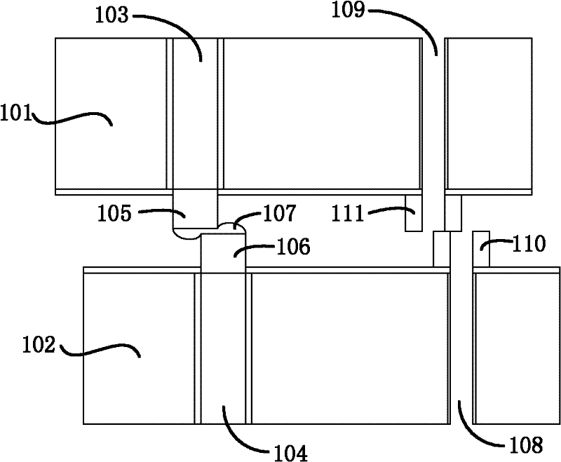
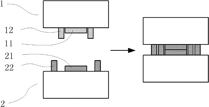
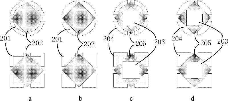
[0031] Specific embodiments of the present invention will be described in detail below in conjunction with the accompanying drawings. It should be noted that the specific embodiments discussed below are only specific embodiments in a specific environment, and do not limit the scope of the present invention. In order to better illustrate the structural characteristics of each layer of silicon chips in the laminated chip of the present invention, all silicon chips in the accompanying drawings are thinned. , The chip is temporarily bonded to the glass, thinned, permanently bonded to the silicon chip, and debonded from the glass. The present invention can be used on other semiconductor chips. The surrounding structures and micro-bumps shown are preferably square and circular, but can also be in any other shape. In addition, the dimensions in the embodiments are for better description of the invention. Not actual scale. The bonding between the metal micro-bumps in the present inv...


PUM


Abstract

The invention discloses a TSV (through silicon via) chip bonding structure, belonging to the technical field of micro electronics. The bonding structure comprises a first chip and a second chip, wherein the first chip comprises a first micro bump and first surrounding structures around the first micro bump; the height of the first surrounding structures is more than that of the first micro bump; the second chip comprises a second micro bump; the second micro bump is embedded into the first surrounding structures and the first surrounding structures restrict lateral displacement of the second micro bump; the second chip also comprises second surrounding structures; and the first surrounding structures are embedded into the second surrounding structures and the second surrounding structuresrestrict lateral displacement of the first surrounding structures. The TSV chip bonding structure can be used in such fields as manufacturing of semiconductor devices and the like.

Description

technical field [0001] The invention relates to a TSV (Through Silicon Via, through-silicon via) chip three-dimensional integration technology, in particular to a design of a TSV bonding layer structure, and belongs to the field of microelectronic technology. Background technique [0002] Today's semiconductor industry generally believes that TSV-based chip three-dimensional integration technology is one of the important technologies that can make chips continue to develop along the blueprint of Moore's Law. For the stacking of TSV chips, one of the common and reliable methods at present is to perform intermetallic bonding between micro bumps (micro bumps) through solder to form an intermetallic compound (IMC). IMC has a higher melting point and can be bonded to another layer of chips. [0003] Such as figure 1 As shown, 101 and 102 are TSV chips, 103 and 104 are conductive vias, and 105 and 106 are conductive micro-bumps. Generally, 105 and 106 are bonded by solder 107 ....

Claims


Application Information

Patent Timeline
Patent Type & Authority Patents(China)
IPC IPC(8): H01L23/00H01L23/48
CPCH01L2224/81385H01L2224/16145
Inventor 崔卿虎朱韫晖马盛林缪旻金玉丰
Owner PEKING UNIV
Why Eureka
Try Eureka