


Quick Research
Generate reliable direction feasibility study reports for your R&D in just a few steps.

Technical Q&A
Discover and master advanced knowledge NOW. Basics, ideas, possibilities, all at once.

Find Solutions
As an expert in R&D theories, this can generate solutions to your technical problems instantly.

Evaluate Feasibility
Analyze your overall solution with one click, know your potential R&D risks in advance.

Monitor Landscape
Get weekly tech updates, stay abreast of the latest tech innovations and key insights.
Current delay circuit
A delay circuit and current technology, applied in the direction of electrical components, adjusting electrical variables, DC power input to DC power output, etc., can solve the problems of delay change, sacrifice area, unfavorable chip integration, etc., to achieve stable delay, The effect of small mirror current error
- Summary
- Abstract
- Description
- Claims
- Application Information
AI Technical Summary
Problems solved by technology
Method used
Image

Examples
Embodiment Construction
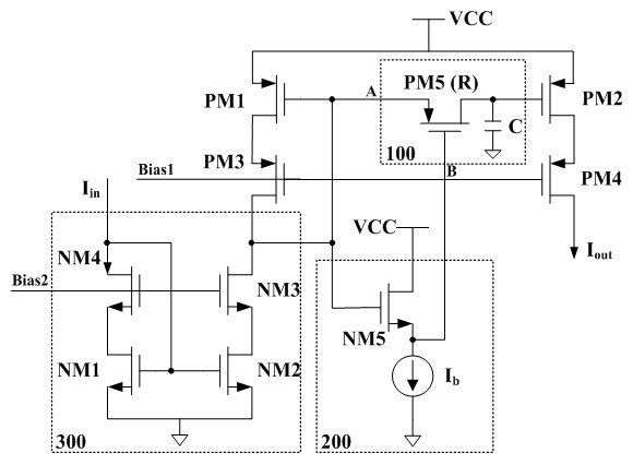
[0010] refer to figure 1 As shown, the current delay circuit of the present invention includes five PMOS transistors (PM1, PM2, PM3, PM4, PM5), five NMOS transistors (NM1, NM2, NM3, NM4, NM5) and a current source I b . Among them, the current input terminal I in The drain of the NMOS transistor NM4, the gate of the NMOS transistor NM1 and the gate of the NMOS transistor NM2 are respectively connected, the gate of the NMOS transistor NM4 is connected to the gate of the NMOS transistor NM3 and the bias voltage Bias2 is connected, and the source of the NMOS transistor NM4 is connected to The drain of the NMOS transistor NM1, the source of the NMOS transistor NM1 are grounded, the source of the NMOS transistor NM2 is grounded, the drain of the NMOS transistor NM2 is connected to the source of the NMOS transistor NM3, and the drains of the NMOS transistor NM3 are respectively connected to the drain of the PMOS transistor PM3 pole, the gate of PMOS transistor PM1, the source of PM...
PUM
 Abstract
Description
Claims
Application Information
 - R&D Engineer
- R&D Manager
- IP Professional
- Industry Leading Data Capabilities
- Powerful AI technology
- Patent DNA Extraction
Browse by: Latest US Patents, China's latest patents, Technical Efficacy Thesaurus, Application Domain, Technology Topic, Popular Technical Reports.
© 2024 PatSnap. All rights reserved.Legal|Privacy policy|Modern Slavery Act Transparency Statement|Sitemap|About US| Contact US: help@patsnap.com