
White LED chip and forming method thereof

A LED chip, white technology, applied in the direction of electrical components, electric solid devices, circuits, etc., can solve the problems of angle change, complex control circuit, unstable color temperature, etc., and achieve the effect of simple control

Inactive Publication Date: 2011-07-20
ENRAYTEK OPTOELECTRONICS
View PDF6 Cites 18 Cited by
  • Summary
  • Abstract
  • Description
  • Claims
  • Application Information

AI Technical Summary

Problems solved by technology

[0006] (1) White light is synthesized by LED red, blue, and yellow three-primary-color multi-chip combination; disadvantages: different light decays of the three primary colors lead to unstable color temperature, complex control circuit, and high cost
[0007] (2) The blue LED chip excites the yellow phosphor powder, and the white light is synthesized by the blue light of the LED and the yellow-green light emitted by the phosphor powder. In order to change the color rendering performance, a small amount of red phosphor powder can be added to it or an appropriate amount of green and red phosphor powder can be added at the same time; Disadvantages: Poor consistency, color temperature, angle variation
Disadvantages: At present, the efficiency of LED chips is low, there are problems of ultraviolet light leakage, and the problem of temperature stability of phosphor powder needs to be solved

Method used


Image

  • White LED chip and forming method thereof
  • White LED chip and forming method thereof
  • White LED chip and forming method thereof

Examples


Embodiment Construction

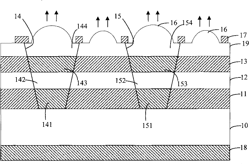
[0070] In the white LED chip and its forming method according to the specific embodiment of the present invention, by forming the first groove and the second groove in the single-color LED chip, the other two kinds of monochromatic LED chips are respectively formed in the first groove and the second groove. When controlling the LED chip to emit light, one LED chip can simultaneously emit three colors of red, green and blue light. After the three colors of light are mixed, it can emit white light, and because it is the control of the same chip, it can be controlled Simple. Moreover, using a silicon substrate whose crystal orientation deviates from 1 to 9° along the (111) crystal plane, and growing a buffer layer on the silicon substrate with the crystal orientation direction, the dislocation between the buffer layer and the silicon substrate can be reduced , reduce the peeling phenomenon between the silicon substrate and the buffer layer, thereby improving the service life of t...


PUM


Abstract

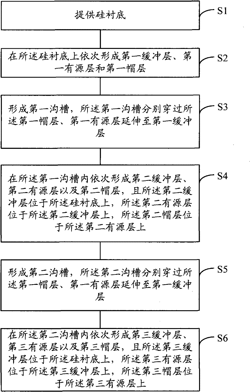
The invention relates to a white light-emitting diode (LED) chip and a forming method thereof. The white LED chip comprises a silicon substrate, a first buffer layer, a first active layer, a first cap layer, a first groove and a second groove, wherein the first buffer layer, the first active layer and the first cap layer are positioned on the silicon substrate sequentially; the first groove passes through the first buffer layer and the first active layer respectively to extend to the first cap layer, and a second buffer layer, a second active layer and a second cap layer are arranged in the first groove; the second groove passes through the first buffer layer and the first active layer respectively to extend to the first cap layer, and a third buffer layer, a third active layer and a third cap layer are arranged in the second groove; and the first active layer, the second active layer and the third active layer are selected from one of a blue light active layer, a green light active layer and a red light active layer respectively and are the active layers with different colors. When used, the white LED chip can emit red light, green light and blue light simultaneously, and can emit white light after the light with three colors is mixed; and due to the adoption of the silicon substrate which deviates 1 to 9 degrees from a crystal plane (111) in the crystal orientation, dislocation between the buffer layers and the silicon substrate can be reduced.

Description

technical field [0001] The invention relates to the field of semiconductor lighting, in particular to a white LED chip and a forming method thereof. Background technique [0002] Semiconductor light-emitting diode, or LED (Light Emitting Diode), is a semiconductor solid-state light-emitting device. It uses a solid semiconductor chip as a light-emitting material. In the semiconductor, the excess energy is released through the recombination of carriers to cause photon emission, and directly emits red, yellow, blue, green, blue, orange, purple and other colors of light. [0003] LEDs are divided into monochrome LEDs and white LEDs according to the color of the light emitted. Ultra-high-brightness LEDs appeared in the 1980s. The substrates of early red LEDs were opaque materials with a luminous efficiency of 1-2 lumens / watt (lumens / watt); they were improved later by using transparent substrates ; Among all ultra-high brightness red LEDs, the efficiency of the best model is abo...

Claims


Application Information

Patent Timeline
IPC IPC(8): H01L27/15H01L33/16H01L33/00
Inventor 张汝京肖德元
Owner ENRAYTEK OPTOELECTRONICS
Learn More