
Method for measuring heat conduction parameter in thin layer material of active area of semiconductor device

A thin-layer material and semiconductor technology, which is applied in the field of semiconductor device testing, can solve the problems of low measurement accuracy, limitation, and inability to measure the heat conduction speed in the thin layer, and achieve the effect of improving the detection sensitivity.

Active Publication Date: 2011-07-20
BEIJING UNIV OF TECH
View PDF3 Cites 5 Cited by
  • Summary
  • Abstract
  • Description
  • Claims
  • Application Information

AI Technical Summary

Problems solved by technology

Due to the time delay in switching from the operating state to the measurement state, combined with the fact that the thin layer material in the active region of new semiconductor devices is very thin, its thermal time constant is usually lower than the measurement delay time, it is difficult to determine the transient heat conduction characteristics in this layer
Other optical methods, such as the Raman method, to measure the temperature rise characteristics of the device are also limited due to cumbersome operations and low measurement accuracy.
In the prior art, the active area acts as a heating area and a temperature detection area at the same time, and the conduction velocity of heat in the thin layer cannot be measured

Method used


Image

  • Method for measuring heat conduction parameter in thin layer material of active area of semiconductor device
  • Method for measuring heat conduction parameter in thin layer material of active area of semiconductor device
  • Method for measuring heat conduction parameter in thin layer material of active area of semiconductor device

Examples


Embodiment Construction

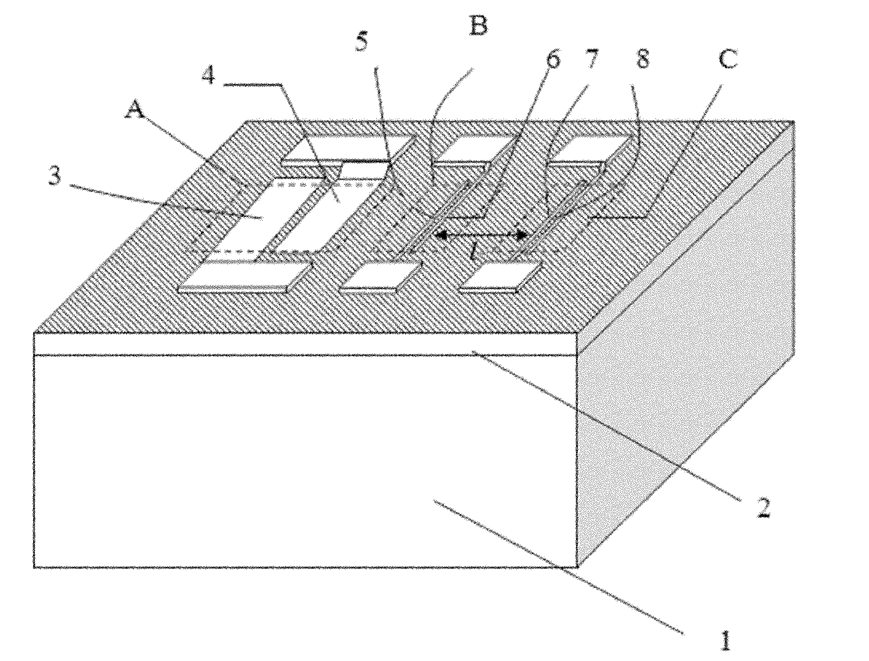
[0019] See figure 1 As shown, a 1.5 micron gallium nitride (GaN) active region thin layer 2 is epitaxially grown on a 400 micron thick silicon carbide (SiC) substrate layer 1 by means of epitaxy. Since the heat source region is used to apply electric power to generate heat, its power The stronger the load capacity, the more conducive to improving the test accuracy. Therefore, the area of ​​the first ohmic contact electrode and the second ohmic contact electrode is required to be larger. The first ohmic contact electrode 3 with a length of 10 microns and a width of 100 microns is prepared by the ohmic contact process. and the third ohmic contact electrode 4 to form a heat source region, using the Schottky junction preparation process to prepare the first Schottky contact electrode 5 and the second Schottky contact electrode 7 with a length of 0.5 microns and a width of 100 microns respectively, The third ohmic contact electrode 6 and the fourth ohmic contact electrode 8 with a ...


PUM


Abstract

The invention discloses a method for measuring a heat conduction parameter in a thin layer material of an active area of a semiconductor device, and relates to the field of semiconductor device test. In the prior art, the active area simultaneously plays the roles of a heating area and a temperature detection area, and the conduction speed of heat in a thin layer cannot be measured. A test chip prepared by adopting the method separates a heat source area and a temperature sensitive detection area on space. Heating and measurement processes can be simultaneously performed, so time delay does not exist, and the measured heat time constant of an actual device structure reaches nanosecond level (based on the speed of a high-speed analog / digital (A / D) acquisition card). The method can fulfill the purpose of testing the heat conduction parameter of the thin layer of the actual active area of the device such as a Schottky gate structure-based device such as a GaN high electron mobility transistor (GaN HEMT) or the like, and can also be used for measuring the heat conduction parameter of a specific film material.

Description

technical field [0001] The invention relates to the field of semiconductor device testing. Background technique [0002] When a semiconductor device is working, the heat generated in the active area will cause the temperature of the chip to rise, which will have a direct impact on the performance parameters of the device, especially the service life and reliability. The thin-layer material in the active region of a semiconductor device is both a heat generating region and a heat conducting region. The conduction speed and thermal time constant of heat in this region are important parameters affecting the thermal performance of the device. Especially for power microwave devices, there is a lot of heat generated and the speed of change is fast, and the impact of transient temperature rise on the device chip has a serious impact on performance. Determining the effect of the heat conduction velocity and thermal time constant in the active region on its performance is critical....

Claims


Application Information

Patent Timeline
Patent Type & Authority Applications(China)
IPC IPC(8): G01R31/26
Inventor 冯士维张光沉郭春生乔彦彬刘静
Owner BEIJING UNIV OF TECH
Learn More