Complementary metal oxide semiconductor (CMOS) active region isolating process

An active area and process technology, applied in electrical components, semiconductor/solid-state device manufacturing, circuits, etc., can solve the problems of reducing the length of the bird's beak, complex process, poor surface morphology, etc. The effect of simple process operation

Inactive Publication Date: 2011-06-22
WUXI ZHONGWEI JINGYUAN ELECTRONIC CO LTD
View PDF1 Cites 0 Cited by
  • Summary
  • Abstract
  • Description
  • Claims
  • Application Information

AI Technical Summary

Problems solved by technology

The Recessed LOCOS isolation technology adopts the method of etching a certain thickness of the Si substrate first, and then performing LOCOS oxidation, which makes this process reduce the length of the bird's beak compared with the usual LOCOS process, and can achieve smaller active region spacing isolation, but Due to the poor surface topography, there is a groove between the active area and the field area, which makes the isolation depth of this process limited, which limits the application of this process
A variety of laterally sealed isolation technologies developed on the basis of these conventional isolation process technologies have alleviated the problem of the bird's beak length of isolation oxidation to a certain extent, but these isolation technologies are either complex in process or have some special common CMOS processes The process conditions that the line does not have make these isolation technologies not have good engineering practicability

Method used


Image

  • Complementary metal oxide semiconductor (CMOS) active region isolating process
  • Complementary metal oxide semiconductor (CMOS) active region isolating process
  • Complementary metal oxide semiconductor (CMOS) active region isolating process

Examples


Embodiment Construction

[0024] The present invention will be further described below in conjunction with specific drawings and embodiments.

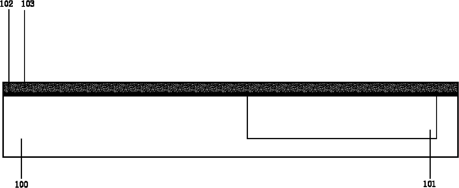
[0025] Such as figure 1 As shown in ~ 10: the present invention includes a first conductivity type substrate 100, a second conductivity type well region 101, a first barrier layer 102, a second barrier layer 103, a photoresist 104, a first spacer layer 105, a second The side wall layer 106 , the side wall 107 , the isolation layer 108 and the buried layer of silicon dioxide 109 .

[0026] In order to isolate the active area of ​​the CMOS device, reduce the bird's beak after isolation and oxidation, reduce the isolation spacing of the active area, and make the field area and the active area flatter, the CMOS active area isolation process includes the following steps:

[0027] a. Provide a first conductivity type substrate 100, and form a second conductivity type well region 101 on the first conductivity type substrate 100, such as figure 1 shown;

[0028] T...


PUM


Abstract

The invention relates to a complementary metal oxide semiconductor (CMOS) active region isolating process. The process comprises the following steps: a, providing a first conductive type substrate, and forming a second conductive type well region; b, arranging a first barrier layer and a second barrier layer on the first conductive type substrate in sequence; c, coating a photoresist, and removing the photoresist on the field; d, removing the second barrier layer and first barrier layer on the field; e, etching the field to form an isolation trench; f, arranging a first side wall layer and a second side wall layer; g, removing the corresponding second side wall layer on the active region and at the bottom of the isolation trench, and forming a correspondingly distributed side wall in the isolation trench; h, oxidizing on the field to form an isolation layer; i, removing the corresponding first side wall layer and second barrier layer on the active region, and removing the side wall which is on the first conductive type substrate and is corresponding to the field; and j, removing the first barrier layer on the first conductive type substrate. The process is easy to operate, and the beak is reduced, so the isolation requirement of a deep sub-micron CMOS process is met.

Description

technical field [0001] The present invention relates to an active area isolation process, in particular to a CMOS active area isolation process, specifically to the active area isolation of bulk silicon CMOS and SOI (Silicon On Insulator) CMOS with a feature size of 0.25 μm and above craft. Background technique [0002] The active interval isolation methods commonly used in CMOS technology are: ordinary LOCOS (LOCal Oxidation of Silicon) isolation, PBL (Poly-Buffered LOCOS) isolation, SPOT (Self-Aligned Planar-Oxidation Technology) isolation, Recessed LOCOS isolation and STI isolation ( shallow trench isolation), etc. In addition to these relatively mature isolation processes, other isolation methods have been continuously proposed, such as lateral sealing LOCOS isolation, SWAMI (SideWAll-Masked I solation Technique), etc. Each isolation technology has its own advantages and disadvantages. [0003] The advantage of ordinary LOCOS isolation is that the process is simple, ...

Claims


Application Information

Patent Timeline
Patent Type & Authority Applications(China)
IPC IPC(8): H01L21/762H01L21/311
Inventor 洪根深顾爱军陈正才李俊
Owner WUXI ZHONGWEI JINGYUAN ELECTRONIC CO LTD
Why Eureka
Try Eureka