
Silicon-based long-wave infrared waveguide and preparation method thereof

A technology of infrared light wave and long wave, applied in the direction of optical waveguide light guide, light guide, optics, etc., can solve the problems of difficult preparation, high equipment requirements, and great difficulty, and achieve good prospects and value, low process difficulty, and simple structure Effect

Inactive Publication Date: 2011-06-15
ZHEJIANG UNIV
View PDF3 Cites 5 Cited by
  • Summary
  • Abstract
  • Description
  • Claims
  • Application Information

AI Technical Summary

Problems solved by technology

This structure is more difficult for the process requirements, and cladding layers of different materials need to be deposited repeatedly; compared with the present invention, the Undercut SOI waveguide structure requires a self-stop process for deep etching, and also requires secondary oxidation on the substrate silicon and secondary lithography, and there is an alignment problem
In addition, due to the need to etch the entire silicon substrate of more than 350um, the thickness of the silicon dioxide layer used as a mask is greatly increased, and the required thickness cannot be achieved only by thermal oxidation, and sputtering and other methods are also required; The freestanding structure waveguide prepared by the beam direct writing method has too high requirements on the equipment, and it is difficult to prepare a larger size, and the loss is relatively large in the application of long-wave infrared

Method used


Image

  • Silicon-based long-wave infrared waveguide and preparation method thereof
  • Silicon-based long-wave infrared waveguide and preparation method thereof
  • Silicon-based long-wave infrared waveguide and preparation method thereof

Examples


Embodiment

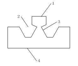
[0062] Taking the wavelength of 10.6um and needing to etch 30um as an example, the side etching length can be obtained by the tangent formula, , by calculating the ratio of the width of the waveguide to the width of the support platform is greater than 2.5, in this example, the width of the waveguide is 5um, the width of the support platform is less than 2um, so the length of the mask is .

[0063] In the process of hollowing out the silicon substrate on the lower end surface of the waveguide, the lower end surface of the waveguide will be eroded to a certain extent due to the erosion effect, and the erosion will stop when it reaches the oxide layer on the side wall of the waveguide. The angle between the erosion surface and the horizontal plane is also 54.7 degrees, so the erosion depth in the vertical direction can be calculated by the tangent formula. In this example, the distance to be hollowed out on one side of the waveguide is 1.5um, so the depth of erosion inside th...


PUM

PropertyMeasurementUnit
thicknessaaaaaaaaaa

Abstract

The invention discloses a silicon-based long-wave infrared waveguide and a preparation method thereof. The preparation method comprises the following steps of: preparing a waveguide structure on a common silicon slice, preparing a silicon dioxide mask by using a thermal oxidation method, and then carrying secondary photoetching; setting windows on both sides of a waveguide, carrying out wet corrosion by using a KOH (Potassium Hydroxide) solution, and realizing etching speeds of different crystal faces by selecting a proper concentration and a temperature; and achieving the purpose of slotting by using side corrosion. The long-wave infrared waveguide prepared in the method has simple structure and low process difficulty and is prepared from the common silicon slice without an expensive SOI slice and realizes back deep etching without stopping a corrosion process. For different wavelengths, low transmission loss can be realized by optimizing structural parameters.

Description

technical field [0001] The invention relates to an integrated optical device, in particular to a silicon-based long-wave infrared (above 3um) optical waveguide structure prepared by a trapezoidal platform supporting an inverted trapezoidal lower end surface based on a wet etching process and a preparation method thereof. Background technique [0002] Since the new century, the IT industry represented by the Internet and the new generation of mobile communication technology has greatly promoted the research and development of integrated optoelectronic devices, and its own development has also promoted their application scope, gradually expanding from the communication field to the industrial , military, energy, medical, biological, sensing and other fields. In particular, silicon-based optoelectronic devices combined with the current mature CMOS technology create the possibility of low-cost, large-scale functionalization and modularization. [0003] At present, the silicon-b...

Claims


Application Information

Patent Timeline
Patent Type & Authority Applications(China)
IPC IPC(8): G02B6/136G02B6/13
Inventor 李国熠魏玉欣周强杨建义王明华江晓清
Owner ZHEJIANG UNIV
Learn More