
Method for forming groove

A trench and wafer technology, used in electrical components, semiconductor/solid-state device manufacturing, circuits, etc., can solve problems such as uneven surface, semiconductor device damage, and deep trench etching, avoiding over-etching problems, The effect of reducing damage and improving quality

Active Publication Date: 2011-05-04
SEMICON MFG INT (SHANGHAI) CORP +1
View PDF10 Cites 1 Cited by
  • Summary
  • Abstract
  • Description
  • Claims
  • Application Information

AI Technical Summary

Problems solved by technology

[0005] But in above-mentioned method, owing to in previous process, for example chemical mechanical polishing (CMP), make the surface of the interlayer dielectric layer on the wafer not flat, in other words, the interlayer dielectric layer of wafer edge region and the layer of wafer central region The thickness of the interlayer is different, so that the depth of the groove in the edge region of the wafer formed by etching is different from the groove in the central region of the wafer, which will easily cause the groove in the edge region of the wafer to be etched too deep, thereby affecting the underlying semiconductor. device damage

Method used


Image

  • Method for forming groove
  • Method for forming groove
  • Method for forming groove

Examples


Embodiment Construction

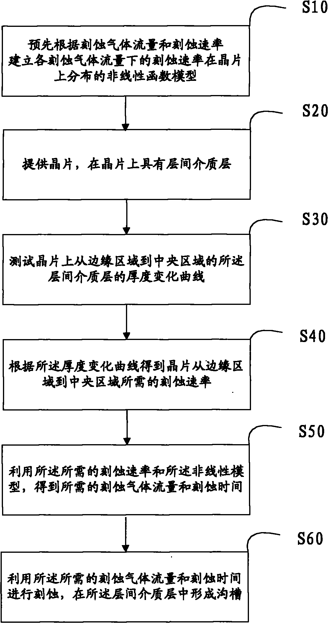
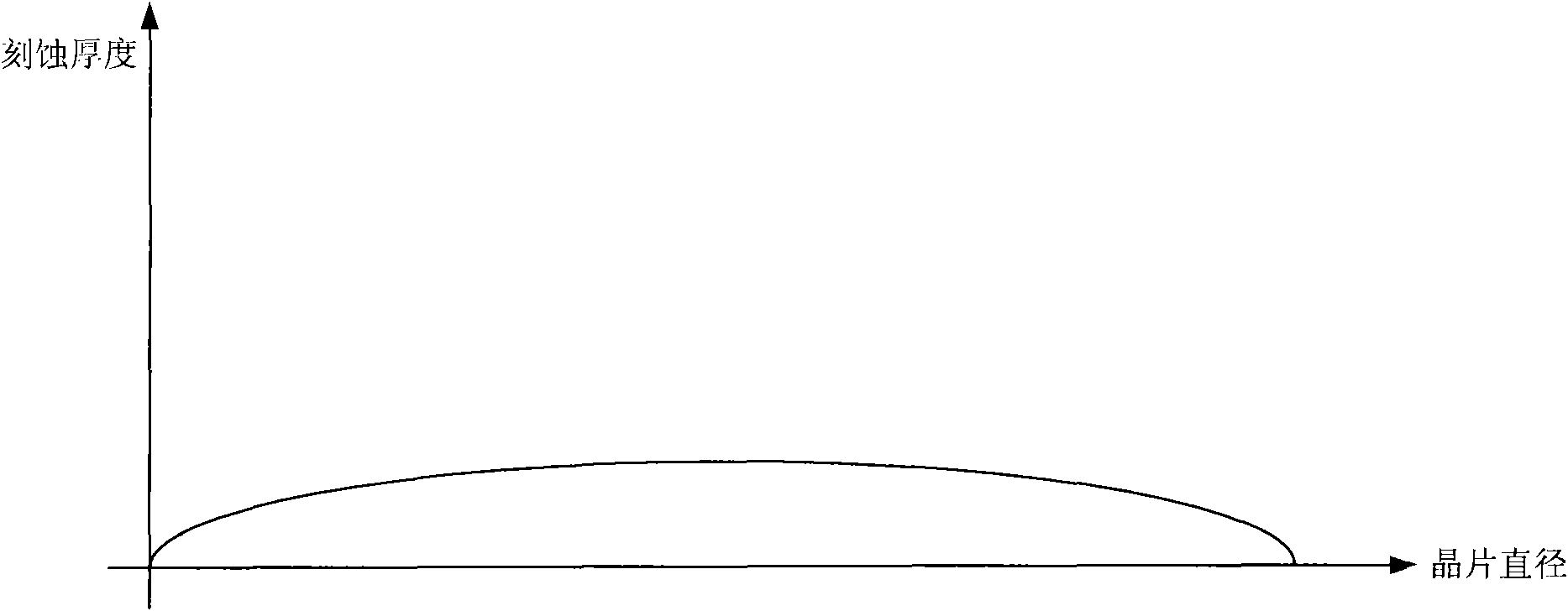
[0027] It can be seen from the background technology that since the thickness of the interlayer dielectric layer in the edge region of the wafer is different from the thickness of the interlayer dielectric layer in the central region of the wafer, the depths of the grooves in the edge region of the wafer formed by etching are different from those in the central region of the wafer. It is easy to etch the trenches in the edge region of the wafer too deeply, thereby causing damage to the underlying semiconductor devices.

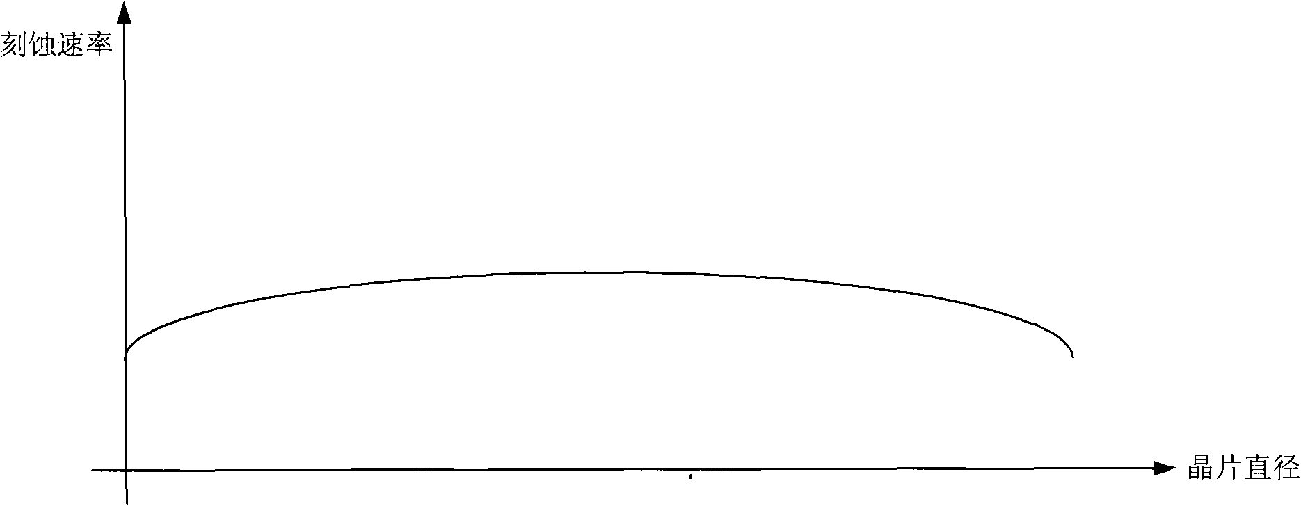
[0028] The inventor of the present invention thinks through a large number of experiments: because the etching gas is not evenly distributed in the etching chamber, usually the distribution of the etching gas flow in the center of the etching chamber and the edge of the etching chamber is different, so that the flow rate of the wafer edge region The etching rate of the interlayer dielectric layer and the interlayer dielectric layer in the wafer central region i...


PUM


Abstract

The invention discloses a method for forming a groove by constructing a nonlinear function model of etching speeds under each etching gas flow distributed on a wafer in advance according to the etching gas flow and the etching speed. The method comprises the steps of: providing the wafer which is provided with an interlayer medium layer; testing a variation curve in thickness of the interlayer medium layer on the wafer from the marginal area to the central area; obtaining etching speeds required from the marginal area to the central area on the wafer based on the variation curve in thickness,gaining required etching gas flow and etching time by utilizing the required etching speed and the nonlinear function model; etching by utilizing the required etching gas flow and the etching time toform a groove in the interlayer medium layer, thereby reducing damages to components under the groove.

Description

technical field [0001] The invention relates to the technical field of semiconductor manufacturing, in particular to a method for forming a groove. Background technique [0002] With the development of integrated circuits to ultra-large-scale integrated circuits, the circuit density inside integrated circuits is increasing, and the number of components contained is also increasing. This development makes the surface of the wafer unable to provide enough area to manufacture the required interconnecting wires. [0003] In order to meet the requirements of interconnection lines after shrinking components, the design of two or more layers of multilayer metal interconnection lines has become a method commonly used in VLSI technology. At present, the conduction between different metal layers or the metal layer and the pad layer is realized through a metal plug, and the formation of the metal plug includes: a dielectric layer between the metal layer and the metal layer or between ...

Claims


Application Information

Patent Timeline
Patent Type & Authority Applications(China)
IPC IPC(8): H01L21/768H01L21/00
Inventor 张海洋孙武尹晓明
Owner SEMICON MFG INT (SHANGHAI) CORP
Learn More