Active component array and detection method
A technology of active components and detection methods, applied in nonlinear optics, instruments, optics, etc., can solve problems such as improvement, waste of liquid crystal display panel scrap rate and cost, and achieve the effect of improving yield
- Summary
- Abstract
- Description
- Claims
- Application Information
AI Technical Summary
Problems solved by technology
Method used
Image
Examples
Embodiment Construction
[0030] In order to make the above-mentioned features and advantages of the present invention more comprehensible, the following specific embodiments are described in detail together with the accompanying drawings.
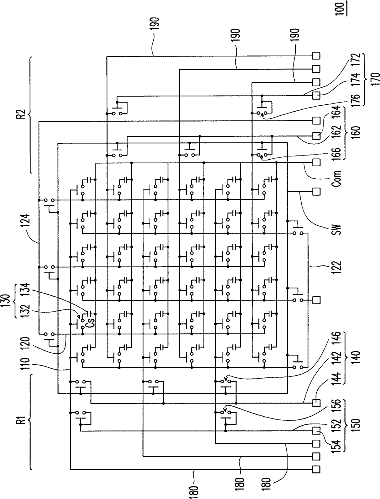
[0031] figure 1 Shown is an active device array according to one embodiment of the present invention. Please refer to figure 1 , the active element array 100 includes a plurality of scanning lines 110, a plurality of data lines 120, a plurality of pixel structures 130, a first detection circuit 140, a second detection circuit 150, a third detection circuit 160 and a fourth detection circuit 170. The scan lines 110 are arranged parallel to each other to define a first region R1 and a second region R2 opposite to each other along the extending direction of the scan lines 110 . In other words, the first region R1 and the second region R2 are respectively located at two opposite ends in the extending direction of the scan line 110 . The extending direction of the d...
PUM
 Abstract
Description
Claims
Application Information
 - R&D
- Intellectual Property
- Life Sciences
- Materials
- Tech Scout
- Unparalleled Data Quality
- Higher Quality Content
- 60% Fewer Hallucinations
Browse by: Latest US Patents, China's latest patents, Technical Efficacy Thesaurus, Application Domain, Technology Topic, Popular Technical Reports.
© 2025 PatSnap. All rights reserved.Legal|Privacy policy|Modern Slavery Act Transparency Statement|Sitemap|About US| Contact US: help@patsnap.com

