Array substrate and manufacturing method thereof
A technology for array substrates and manufacturing methods, applied in the field of liquid crystal displays, can solve problems such as complex production of array substrates, achieve the effects of reducing production costs and improving production efficiency
- Summary
- Abstract
- Description
- Claims
- Application Information
AI Technical Summary
Problems solved by technology
Method used
Image

Examples
Embodiment 1
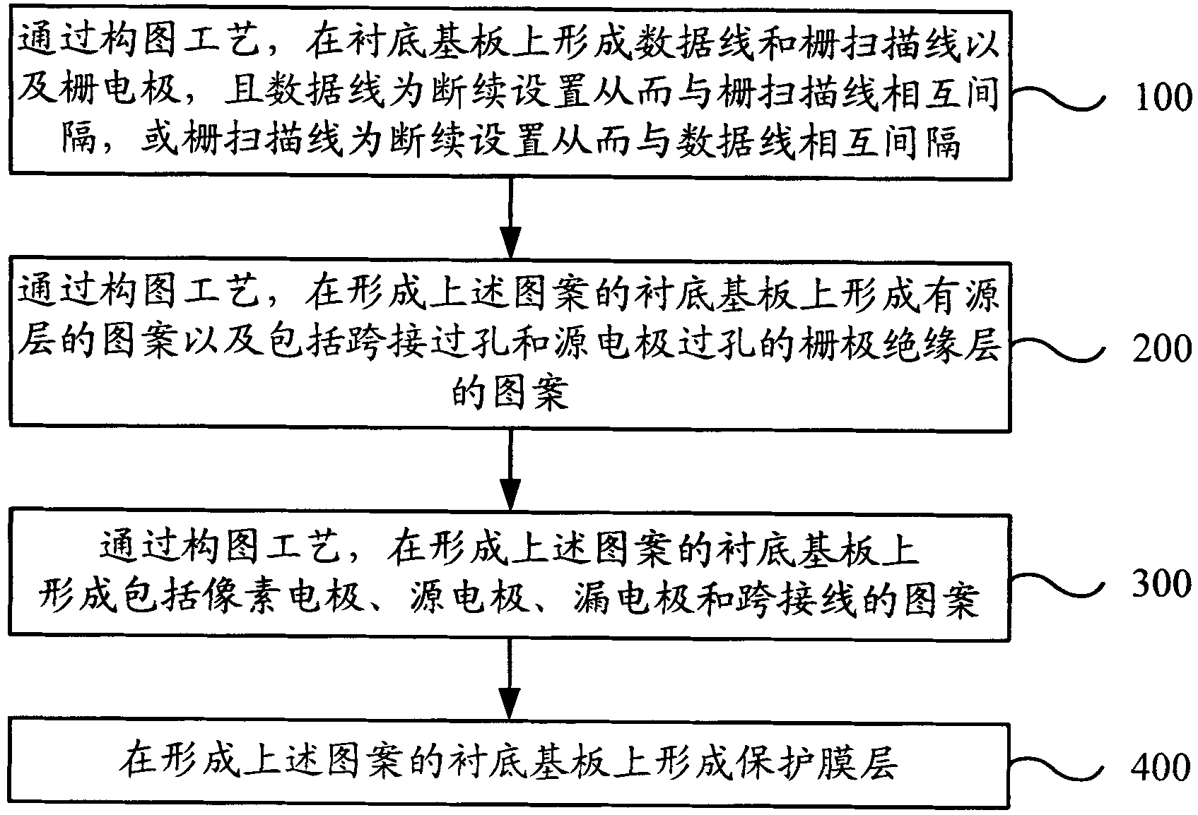
[0035] figure 1 It is a flow chart of an array substrate manufacturing method provided in Embodiment 1 of the present invention, and the method includes the following steps:
[0036] Step 100. Through a patterning process, a pattern including data lines, gate scan lines and gate electrodes intersecting horizontally and vertically is formed on the base substrate, and the data lines are intermittently arranged so as to be spaced from the gate scan lines, or the gate scan lines are Discontinuously set so as to be spaced from the data line;
[0037] Step 200, through a patterning process, form the pattern of the active layer and the pattern of the gate insulating layer including the bridging via hole and the source electrode via hole on the base substrate on which the above pattern is formed, and the position of the bridging via hole corresponds to intermittent And the position of the adjacent data line or gate scanning line, the position of the source electrode via hole correspo...
Embodiment 2
[0048] figure 2 It is a flow chart of the array substrate manufacturing method provided by Embodiment 2 of the present invention. This embodiment can be based on Embodiment 1, and the specific process is as follows:
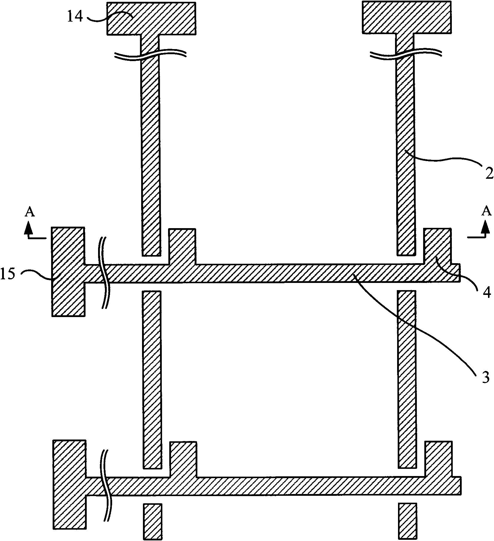
[0049] In step 100, a pattern including data lines 2 , gate scan lines 3 and gate electrodes 4 that intersect horizontally and vertically on the base substrate 1 is formed through a patterning process, specifically including:
[0050] Step 110 , depositing a metal thin film on the base substrate 1 . Specifically, this step can be as follows: use a transparent glass substrate or quartz as the base substrate 1, and deposit a layer with a thickness of 500-4000 angstroms on the base substrate 1 by sputtering or thermal evaporation. The material of the metal film can be any one of chromium (Cr), tungsten (W), titanium (Ti), tantalum (Ta), molybdenum (Mo), aluminum (Al) and copper (Cu) or A multilayer metal thin film composed of multiple metals may also be an allo...
Embodiment 3
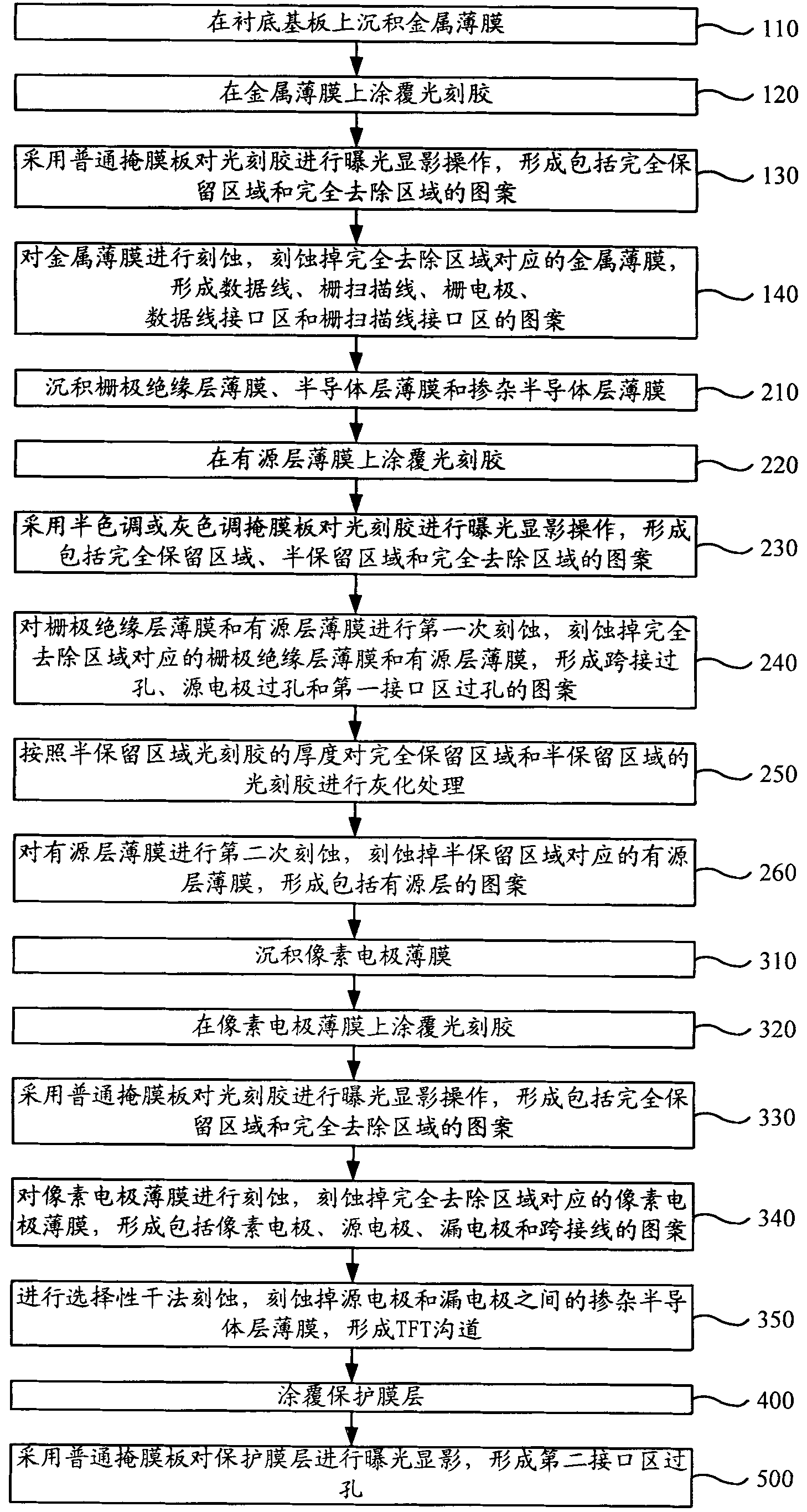
[0081] Figure 9 The flow chart of the array substrate manufacturing method provided by the third embodiment of the present invention, this embodiment may be based on the first embodiment, including the following process:
[0082] Step 110, depositing a film with a thickness of 500-4000 angstroms on the base substrate 1 by sputtering or thermal evaporation metal film;
[0083] Step 120, coating photoresist on the metal film;
[0084] Step 130, using a common mask to expose and develop the photoresist to form a pattern including a completely reserved area and a completely removed area;
[0085]Step 140: Etching the metal thin film, etching away the metal thin film corresponding to the completely removed area, forming a pattern including at least the data line 2, the gate scan line 3 and the gate electrode 4, or forming the data line interface area 14 and the gate electrode 4 at the same time. The pattern of the scan line interface area 15 . In this embodiment, the formatio...
PUM
 Abstract
Description
Claims
Application Information
 - R&D Engineer
- R&D Manager
- IP Professional
- Industry Leading Data Capabilities
- Powerful AI technology
- Patent DNA Extraction
Browse by: Latest US Patents, China's latest patents, Technical Efficacy Thesaurus, Application Domain, Technology Topic.
© 2024 PatSnap. All rights reserved.Legal|Privacy policy|Modern Slavery Act Transparency Statement|Sitemap