Non-volatile memory device as well as non-volatile memory and manufacturing method thereof

A technology of non-volatile storage and manufacturing method, applied in the field of non-volatile storage devices, can solve the problems of difficulty in further shrinking, low manufacturability yield, etc. The effect of programming voltage requirements

Inactive Publication Date: 2011-04-20
SEMICON MFG INT (SHANGHAI) CORP +1
View PDF0 Cites 0 Cited by
  • Summary
  • Abstract
  • Description
  • Claims
  • Application Information

AI Technical Summary

Problems solved by technology

Such devices are limited by difficult further scaling and low manufacturability yields

Method used


Image

  • Non-volatile memory device as well as non-volatile memory and manufacturing method thereof
  • Non-volatile memory device as well as non-volatile memory and manufacturing method thereof
  • Non-volatile memory device as well as non-volatile memory and manufacturing method thereof

Examples


Embodiment Construction

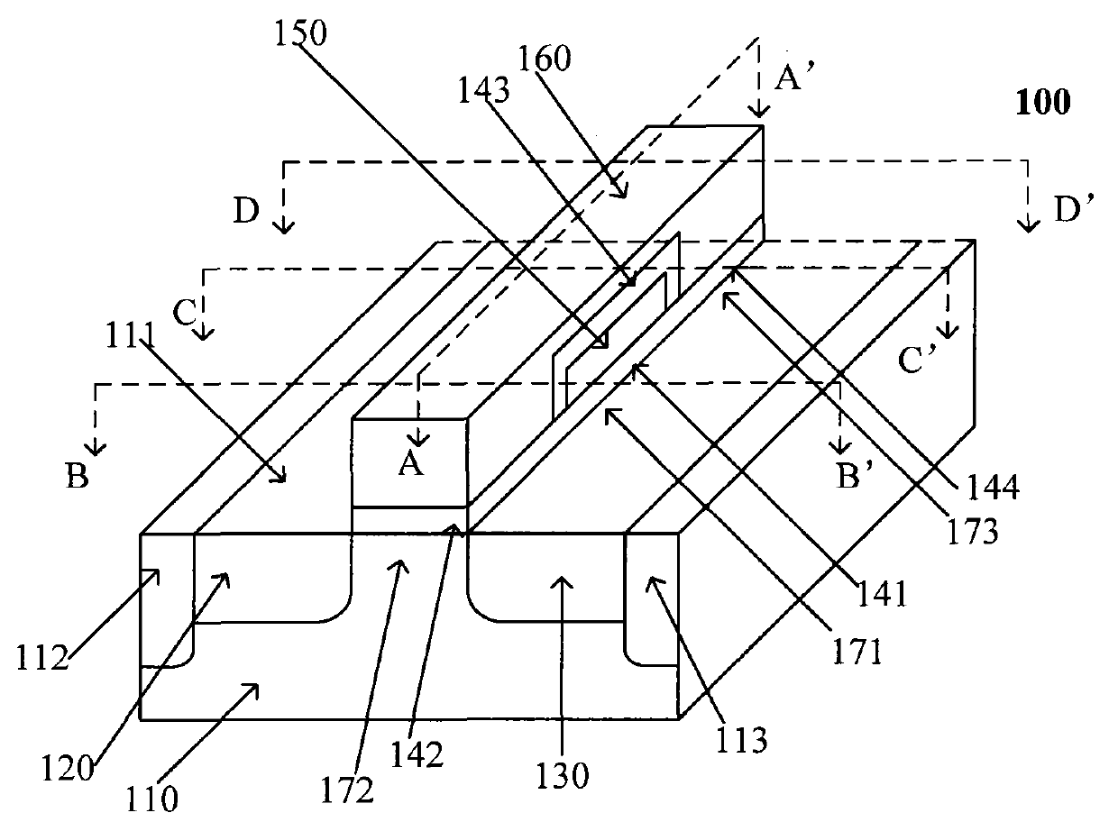
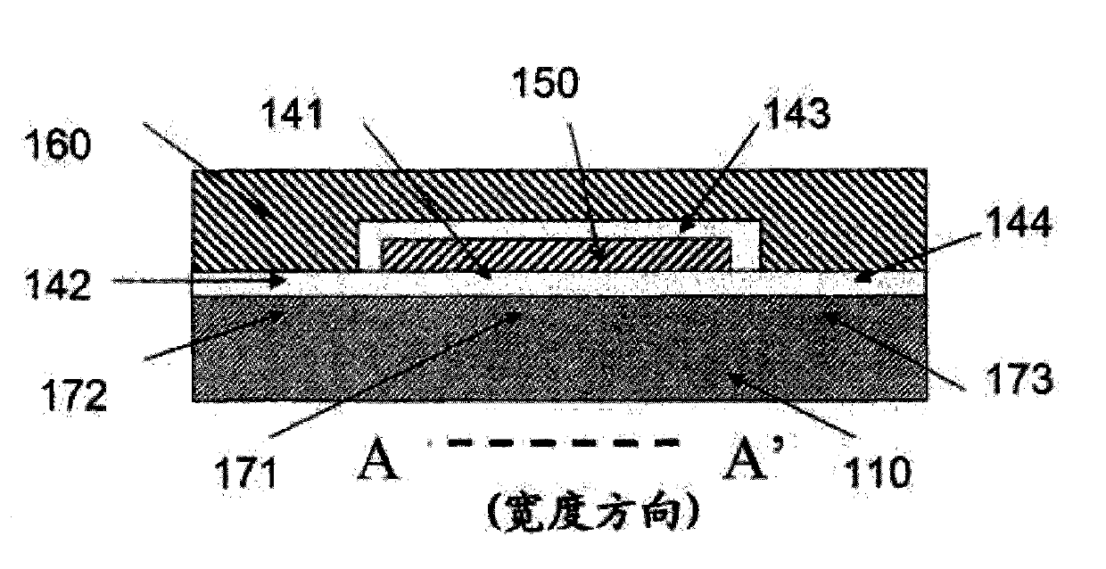
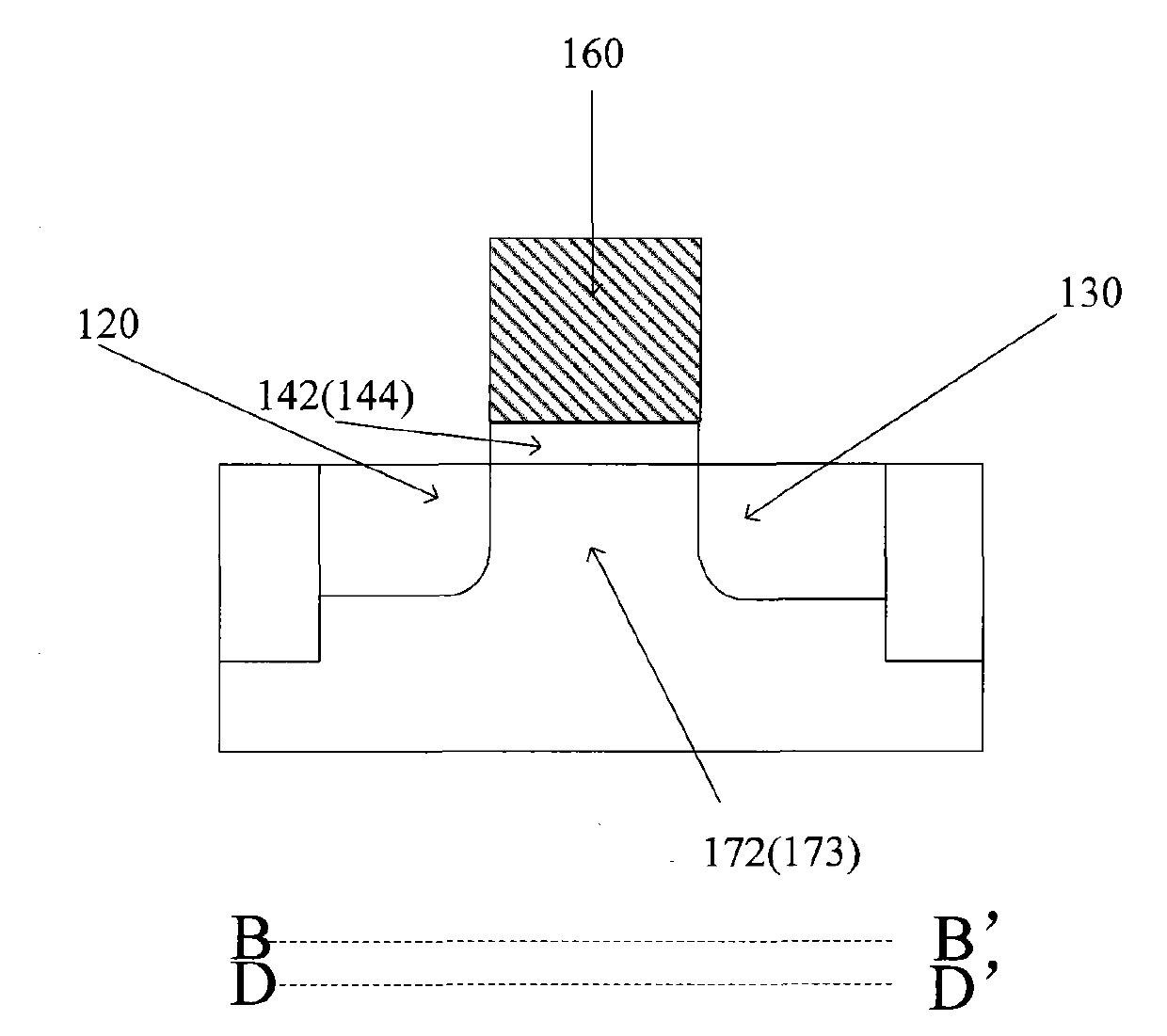
[0037] It can be seen from the background art that the existing non-volatile memory devices have many disadvantages, for example, when the logic devices are adjusted and designed to work at lower voltages, the non-volatile memory devices are difficult to scale down, and high voltage is still required. voltage to operate. For example, existing stacked nonvolatile memory devices require only a single transistor per cell, but require high programming currents, making it difficult to program and erase using on-chip high voltage generation. Existing split-gate nonvolatile memory devices are single-transistor electrically programmable and rewritable memory cells. Erasing of the cell is accomplished by the Fowler-Nordheim tunneling mechanism from the floating gate through the second insulating layer to the control gate. Electrons from the source migrate through the channel region below the control gate and are injected into the floating gate through the first insulating layer due to...


PUM


Abstract

The invention relates to a non-volatile memory device as well as a non-volatile memory and a manufacturing method thereof, wherein the non-volatile memory comprises a semiconductor substrate, and the semiconductor substrate comprises a surface region, a source region positioned in the semiconductor substrate, a drain region positioned in the semiconductor substrate, a first channel region positioned in the semiconductor substrate, a second channel region positioned in the semiconductor substrate, a first dielectric layer covering the first channel region, a second dielectric layer covering the second channel region, a floating gate structure covering the first dielectric layer on the first channel region, a third dielectric layer positioned on the floating gate structure and a control gate layer covering the second dielectric layer and the third dielectric layer, wherein the first channel region extends between a first part of the source region and a first part of the drain region; and the second channel region extends between a second part of the source region and a second part of the drain region. With the adoption of the invention, the high manufacturable yield of the non-volatile memory with low scale can be improved.

Description

technical field [0001] The invention relates to the field of semiconductor manufacturing, in particular to a nonvolatile storage device, a nonvolatile storage device and a manufacturing method thereof. Background technique [0002] Integrated circuits, or "ICs," have grown from a handful of interconnected devices fabricated on a single silicon chip to millions of devices. Current ICs offer performance and complexity far beyond what was originally imagined. To achieve improvements in complexity and circuit density (ie, the number of devices that can be packed onto a given chip area), the size of the smallest device feature, also known as device "geometry," has become smaller with each IC generation. Semiconductor devices are now manufactured with features smaller than a quarter of a micron in cross-section. [0003] Increased circuit density not only improves the complexity and performance of ICs, but also provides lower priced components to consumers. IC manufacturing equ...

Claims


Application Information

Patent Timeline
Patent Type & Authority Applications(China)
IPC IPC(8): H01L27/115H01L29/10H01L29/423H01L21/8247
CPCH01L29/66825H01L29/42324H01L21/28273H01L29/7885H01L29/40114
Inventor 肖德元陈国庆李若加
Owner SEMICON MFG INT (SHANGHAI) CORP
Why Eureka
Try Eureka