


Quick Research
Generate reliable direction feasibility study reports for your R&D in just a few steps.

Technical Q&A
Discover and master advanced knowledge NOW. Basics, ideas, possibilities, all at once.

Find Solutions
As an expert in R&D theories, this can generate solutions to your technical problems instantly.

Evaluate Feasibility
Analyze your overall solution with one click, know your potential R&D risks in advance.

Monitor Landscape
Get weekly tech updates, stay abreast of the latest tech innovations and key insights.
Resistance-variable gating device with high voltage-withstanding self-current limiting performance and preparation method thereof
A gating device, high withstand voltage technology, applied in the direction of electrical components, etc., to achieve the effect of high resistance state stability, low cost, and easy operation
- Summary
- Abstract
- Description
- Claims
- Application Information
AI Technical Summary
Problems solved by technology
Method used
Image

Examples
Embodiment 1
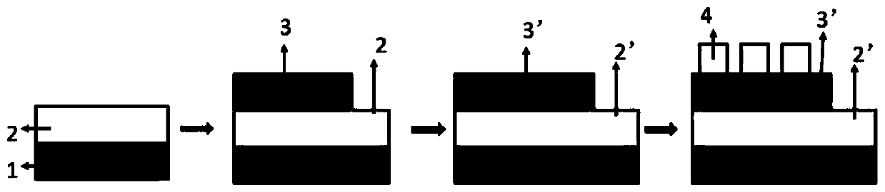
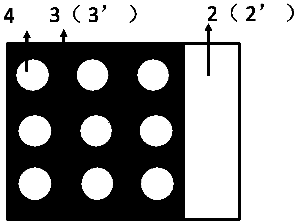
[0057] This embodiment provides a resistive switching gate with high withstand voltage and self-limiting current performance. The structure includes a glass substrate, a bottom electrode thin film nickel, a functional layer hafnium oxide film and a top electrode thin film nickel arranged in sequence from the bottom to the top. The surface of the nickel film on the top electrode is distributed in a cylindrical lattice, and the diameter of the bottom surface of the cylindrical lattice is 30 μm. The area of the nickel film on the bottom electrode is larger than the area of the hafnium oxide film on the functional layer. The thicknesses of the bottom and bottom electrode film nickel, the functional layer film hafnium oxide and the top electrode film nickel are respectively 1mm, 500nm, 300nm, and 500nm; figure 1 Shown is the preparation flow chart of the resistance variable gate, and the specific steps include:
[0058] (1) Substrate pretreatment:
[0059] Soak the glass subst...
Embodiment 2
[0076] This embodiment provides a resistive switching gate with high withstand voltage self-limiting performance. The structure includes a single crystal silicon substrate, a bottom electrode thin film copper nanowire, a functional layer thin film cuprous oxide and The top electrode film is platinum, the surface of the top electrode film nickel is distributed in a lattice pattern, and the diameter of the lattice is 30 μm, and the area of the bottom electrode copper nanowire film is larger than the area of the functional layer cuprous oxide film; the single The thicknesses of the crystalline silicon substrate, the bottom electrode film copper nanowire, the functional layer film cuprous oxide, and the top electrode film platinum are 1mm, 3000nm, 10nm, and 100nm; figure 1 Shown is the preparation flow chart of the resistance variable gate, and the specific steps include:
[0077] (1) Substrate pretreatment:
[0078] Soak the substrate in detergent water, deionized water, abs...
Embodiment 3
[0095] This embodiment provides a resistive switching gate with high withstand voltage and self-limiting current performance. The structure includes a quartz substrate, a bottom electrode thin film of platinum, a functional layer of bismuth telluride thin film and a top electrode thin film of platinum. , the surface of the top electrode film nickel is distributed in a lattice pattern, and the lattice diameter is 30 μm, and the area of the bottom electrode film platinum is greater than the area of the functional layer film bismuth telluride; the quartz substrate, bottom electrode film platinum The thicknesses of the bismuth telluride thin film of the functional layer and the platinum thin film of the top electrode are 1mm, 100nm, 300nm, and 100nm respectively; figure 1 Shown is the preparation flow chart of the resistance variable gate, and the specific steps include:
[0096] (1) Substrate pretreatment:
[0097] Soak the substrate in detergent water, deionized water, abso...
PUM
| Property | Measurement | Unit |
|---|---|---|
| Thickness | aaaaa | aaaaa |
| Thickness | aaaaa | aaaaa |
| Thickness | aaaaa | aaaaa |
Abstract
Description
Claims
Application Information
 - R&D Engineer
- R&D Manager
- IP Professional
- Industry Leading Data Capabilities
- Powerful AI technology
- Patent DNA Extraction
Browse by: Latest US Patents, China's latest patents, Technical Efficacy Thesaurus, Application Domain, Technology Topic, Popular Technical Reports.
© 2024 PatSnap. All rights reserved.Legal|Privacy policy|Modern Slavery Act Transparency Statement|Sitemap|About US| Contact US: help@patsnap.com