Multilayer anti-reflection film for solar cell and preparation method thereof
A technology of solar cells and manufacturing methods, which is applied in the manufacture of circuits, electrical components, final products, etc., can solve problems such as inability to achieve effects, achieve optical matching and electrical passivation, simple preparation process, and low equipment cost.
- Summary
- Abstract
- Description
- Claims
- Application Information
AI Technical Summary
Problems solved by technology
Method used
Image
Examples
Embodiment 1
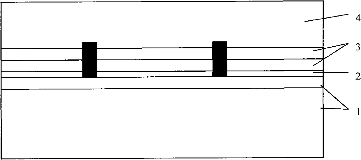
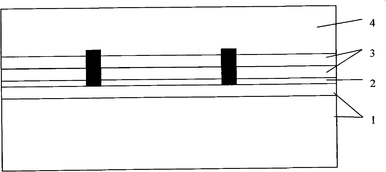
[0019] like figure 1 As shown, the present invention provides a multilayer anti-reflection film for solar cells, comprising SiO 2 film 2 and anti-reflection film 3, the SiO 2 The film 2 is arranged on the solar cell window layer 1, and the anti-reflection film 3 is arranged on the SiO 2 film 2, wherein: the SiO 2 The thickness of the film 2 is 5-40 nm; the thickness of the anti-reflection film 3 is 50-100 nm, and is a light-transmitting film with a refractive index of about 2.3-2.4.
[0020] The anti-reflection film 3 can be made of TiO 2 / SiO 2 Bilayer film, also MgF / TiO 2 / SiO 2 , or SiC / TiO 2 / SiO 2 , SiNx / TiO 2 / SiO 2 , ZnO / TiO 2 / SiO 2 etc. in the form of multilayer films. In this embodiment, as figure 1 As shown, the antireflection film 3 is in the form of a bilayer film.
[0021] The anti-reflection film 3 is covered with EVA 4 . EVA is a plastic material composed of ethylene (E) and vinyl acetate (VA).
[0022] In the solar cell window layer (the cell'...
Embodiment 2
[0024] The manufacturing method of the multilayer antireflection film of the solar cell described in Example 1:
[0025] After the silicon wafers have undergone the normal process of making solar cells, such as texturing, diffusion, and phosphorus washing, thermal oxidation or sol-gel methods are used. + A layer of SiO with a thickness of 5 to 40 nm is grown 2 membrane. Then in SiO 2 An anti-reflection film of 50-100 nm is deposited on the film. After that, the anti-reflection film is covered with EVA and glass encapsulation, and this encapsulation process is a common process.
[0026] In this embodiment, the anti-reflection film is a light-transmitting film with a refractive index of about 2.3, and TiO can be used 2 / SiO 2 bilayer membranes, such as figure 1 shown in.
Embodiment 3
[0028] The manufacturing method of the multilayer antireflection film of the solar cell described in Example 1:
[0029] After the silicon wafer has undergone normal texturing, diffusion, phosphorus washing and other solar cell preparation processes, thermal oxidation or sol-gel methods are used to form the P in the window layer of the solar cell. + A layer of SiO with a thickness of 5 to 40 nm is grown 2 membrane. Then in SiO 2 An anti-reflection film of 50-100 nm is deposited on the film. After that, the anti-reflection film is covered with EVA and glass encapsulation, and this encapsulation process is a common process.
[0030]In this embodiment, the anti-reflection film is a light-transmitting film with a refractive index of about 2.4. In order to achieve the best optical matching, it is in the form of a multi-layer film, which is MgF / TiO 2 / SiO 2 , SiC / TiO 2 / SiO 2 , SiNx / TiO 2 / SiO 2 , ZnO / TiO 2 / SiO 2 one of the others.
[0031] In the present invention, the...
PUM
 Abstract
Description
Claims
Application Information
 - R&D
- Intellectual Property
- Life Sciences
- Materials
- Tech Scout
- Unparalleled Data Quality
- Higher Quality Content
- 60% Fewer Hallucinations
Browse by: Latest US Patents, China's latest patents, Technical Efficacy Thesaurus, Application Domain, Technology Topic, Popular Technical Reports.
© 2025 PatSnap. All rights reserved.Legal|Privacy policy|Modern Slavery Act Transparency Statement|Sitemap|About US| Contact US: help@patsnap.com


