Method for manufacturing electronic component device

A technology for electronic components and manufacturing methods, applied in the fields of electrical components, printed circuit manufacturing, semiconductor/solid-state device manufacturing, etc., can solve problems such as failure to reach the bonding state, and achieve the effects of improving efficiency, reducing costs, and improving productivity

Active Publication Date: 2012-03-28
MURATA MFG CO LTD
View PDF3 Cites 0 Cited by
  • Summary
  • Abstract
  • Description
  • Claims
  • Application Information

AI Technical Summary

Problems solved by technology

In this case, once the applied thickness of metal nanoparticle paste 1 is not enough, Figure 11 In the process of (3), a good bonding state can be obtained on the substrate-side electrode 12 at the highest position, but a sufficient bonding state cannot be achieved on the substrate-side electrode 12 at the lowest position.

Method used


Image

  • Method for manufacturing electronic component device
  • Method for manufacturing electronic component device
  • Method for manufacturing electronic component device

Examples


Embodiment Construction

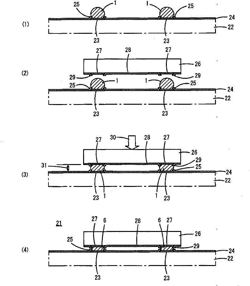
[0072] figure 1 It is explanatory drawing of 1st Embodiment of this invention. figure 1 Representative steps included in the manufacturing method of the electronic component device are shown in figure 1 (4) shows the obtained electronic device 21 .

[0073] First, if figure 1 As shown, a wiring substrate 22 as a first electronic component is prepared. The wiring substrate 22 is constituted by, for example, a resin substrate such as a glass epoxy substrate, a sintered substrate such as an alumina substrate, a Si substrate, or the like. Several substrate-side electrodes 23 are formed on the upper surface of the wiring substrate 22 , and a protective film 24 is formed on substantially the entire upper surface of the wiring substrate 22 . A part of the protective film 24 overlaps the peripheral portion of the substrate-side electrode 23 , thereby forming a bank 25 around the substrate-side electrode 23 . The banks 25 are used to prevent the diffusion of the metal nanopart...


PUM


Abstract

This object aims to provide a method for manufacturing an electronic component device, in which a chip component is mounted on a wiring board, with high productivity and stabilized quality and at a reduced cost. For the purpose, paste (1) of metal nano-particles is applied onto a substrate side electrode (23), a load (30) is applied in such a state that a wiring board (22) is aligned with a chip component (26), whereby compression deforming of the paste (1) of metal nano-particles is performed until the paste becomes a compressive deformation limit thickness (31). Thereafter, the paste (1) ofmetal nano-particles is so heated as to obtain a bonding sintered body (6) made of sintered metal nano-particles, thereby mutually bonding the substrate side electrode (23) and a chip side electrode (27).

Description

technical field [0001] The present invention relates to a method of manufacturing an electronic device comprising a plurality of electronic devices with electrodes joined to each other, and more particularly to a method of manufacturing an electronic device using a metal nanoparticle paste containing metal nanoparticles for bonding between electrodes. Background technique [0002] In recent years, along with the miniaturization of electronic devices, the demand for high integration of semiconductor packages has become stronger. In the mounting technology for mounting and fixing semiconductor packages on wiring boards to achieve electrical conduction, products with high integration and high density are required. [0003] Therefore, a so-called BGA (Ball Grid Array) bonding method in which solder balls are arranged in a grid on the entire back surface of a semiconductor package has attracted attention and has been put into practical use. As mentioned above, since the semicond...

Claims


Application Information

Patent Timeline
Patent Type & Authority Patents(China)
IPC IPC(8): H01L21/60H01L21/56
CPCH01L2224/05573H01L2224/1131H01L2224/13344H01L2224/13339H01L2924/0105H01L2924/01082H01L2224/81193H01L2924/01004H01L2224/97H01L2224/81203H01L24/13H01L23/295H01L2224/16H01L2224/13355H01L2924/01029H01L2924/00013H01L2224/8184H01L2224/13294H05K2201/0257H05K2201/10674H01L2924/01013H01L2224/81191H01L2224/32225H01L24/97H01L2224/81055H01L24/81H01L2924/01047H01L2224/141H01L2924/01079H01L2224/73204H01L2224/81194H05K3/321H01L2924/01005H01L2924/01033H01L24/11H01L2924/01006H01L2224/81192H05K2203/1131H01L2224/16225H01L2224/13347H01L2224/0401H01L2224/05624H01L2224/05644H01L2224/05647H01L2224/06102H01L2924/181H01L2924/00H01L2224/81H01L2224/29099H01L2924/00012H01L2924/00014H01L2924/013H01L2924/01014
Inventor 舟木达弥久米宗一
Owner MURATA MFG CO LTD
Why Eureka
Try Eureka