
Antimony-rich Si-Sb-Te sulfur group compound phase-change material for phase change memory

A phase change memory, chalcogenide technology, applied in metal material coating process, ion implantation plating, coating and other directions, can solve the problem of low transition temperature, high current, and influence on the adhesion of phase change films to electrodes and other films. Additional problems, to achieve the effect of reducing write operation current, improving thermal stability, improving reliability and cycle times

Inactive Publication Date: 2010-12-22
SHANGHAI INST OF MICROSYSTEM & INFORMATION TECH CHINESE ACAD OF SCI
View PDF6 Cites 8 Cited by
  • Summary
  • Abstract
  • Description
  • Claims
  • Application Information

AI Technical Summary

Problems solved by technology

Although Ge 2 Sb 2 Te 5 The data of the memory as a storage medium can be kept for ten years at room temperature, but due to the relatively low transition temperature (about 170 degrees) of the material from the amorphous state to the crystalline state of the cubic structure, there is still a danger that the data cannot be effectively retained. Therefore, increasing the crystallization temperature of the material to improve the thermal stability of the material and thereby enhancing the data retention capacity of the memory has become an urgent problem to be solved.
At the same time due to the use of Ge 2 Sb 2 Te 5 The phase change memory requires a large current when writing, so it is difficult to be widely used in portable products
In addition, during the cyclic transformation process of the amorphous state and the crystalline state of the phase change memory, the thickness of the phase change material film will change. If the change is too large, it will affect the adhesion of the phase change film to electrodes and other film layers. , which is not conducive to the long-term stable operation of the device, and the Ge 2 Sb 2 Te 5 Thin films also have this problem

Method used

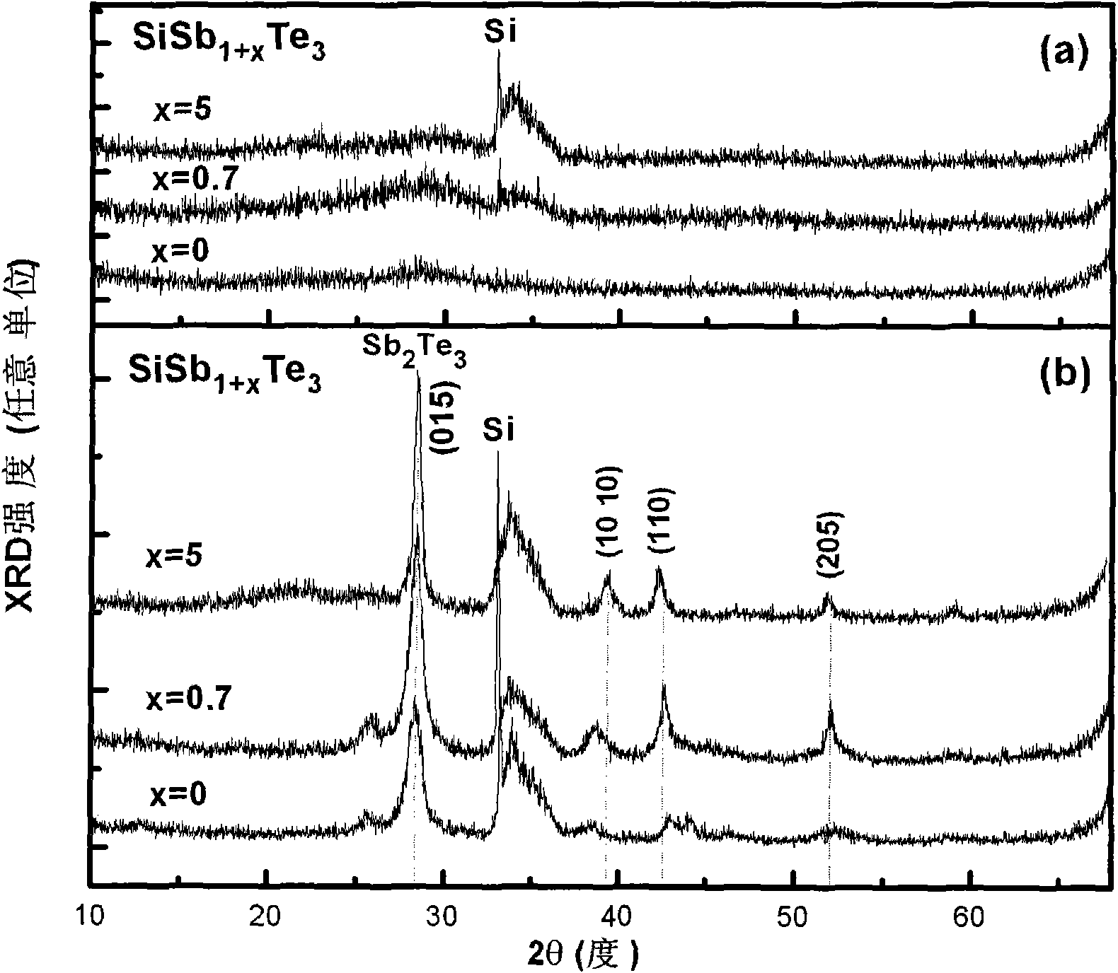
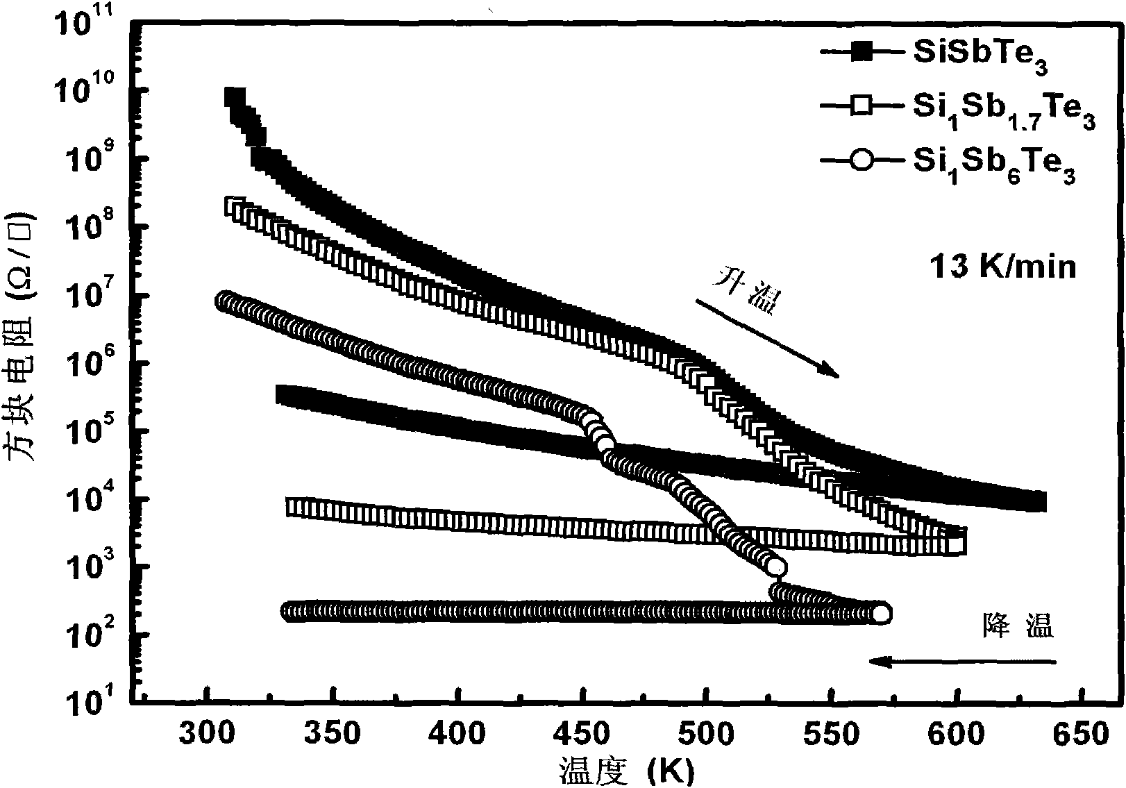
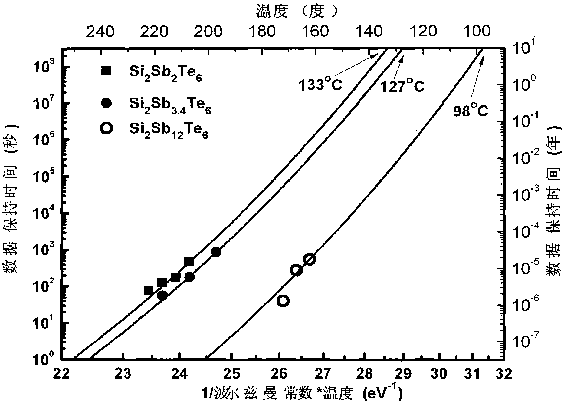

Image

  • Antimony-rich Si-Sb-Te sulfur group compound phase-change material for phase change memory
  • Antimony-rich Si-Sb-Te sulfur group compound phase-change material for phase change memory
  • Antimony-rich Si-Sb-Te sulfur group compound phase-change material for phase change memory

Examples


Embodiment Construction

[0016] The antimony-rich Si-Sb-Te chalcogenide phase-change material for phase-change memory of the present invention has a component general formula of Si a Sb- (100-4a) Te 3a , where 10≤a≤20, which can be formed by various methods, for example, sputtering, electron beam evaporation, vapor deposition, atomic layer deposition, and the like. When sputtering is used, the various elements in the material (i.e. Si, Sb, and Te) can correspond to different targets, and the composition of the material can be controlled by applying different powers to each target, and the thickness of the material can be controlled. It can be controlled by adjusting the sputtering time; it is also possible to prepare a chalcogenide alloy target of the corresponding composition first, and then obtain a thin film of the corresponding composition by sputtering the alloy target, that is, to form a Si-Sb alloy target and a Te elemental target by co-sputtering , or formed by co-sputtering of Si-Te alloy t...


PUM

PropertyMeasurementUnit
thicknessaaaaaaaaaa

Abstract

The invention provides an antimony-rich Si-Sb-Te sulfur group compound phase-change material for a phase change memory, belonging to the technical field of micro-electronics. The phase-change material maintains an atomic ratio of Si to Te of 1:3, the component general formula is SiaSb (100-4a) Te3a, wherein a is more than or equal to 10 and less than or equal to 20; compared with the existing Ge2Sb2Te5, the material features high crystallization temperature, good heat stability and better data retention capacity; moreover, the compound phase-change material in the crystalline state enjoys higher electrical resistivity and small thickness change of the material in crystalline state / amorphous state. With the phase-change material of the invention as the information memory medium, cycle operation times of the memory can be effectively increased, write operation power dissipation can be lowered and device reliability can be improved.

Description

technical field [0001] The invention relates to a phase-change material for a phase-change memory, in particular to an antimony-rich Si-Sb-Te chalcogenide phase-change material for a phase-change memory. Background technique [0002] Memory occupies an important position in the semiconductor market, and phase-change memory, as the most potential next-generation non-volatile memory, uses phase-change thin film materials as storage media to realize information storage, and has become increasingly popular due to its broad application prospects. Become a research hotspot (Tech.Dig.-Int.Electron Devices Meet.2001, 803). Phase-change memory is a memory based on the Ovshinsky electronic effect proposed by S.R.Ovshinsky in the late 1960s (Ovshinsky S R. Reversible electrical switching phenomenon in discovered structure. Phys. Rev. Lett., 1968, 21(20): 1450), which uses the difference in resistance of phase change materials when they undergo reversible transitions between amorphous ...

Claims


Application Information

Patent Timeline
Patent Type & Authority Applications(China)
IPC IPC(8): H01L45/00C23C14/34C23C14/06
Inventor 周夕淋吴良才宋志棠饶峰
Owner SHANGHAI INST OF MICROSYSTEM & INFORMATION TECH CHINESE ACAD OF SCI
Learn More