Method for improving fidelity of Si/Ge emitter window graph

An emitter, fidelity technology, applied in the photoengraving process of the pattern surface, the original for opto-mechanical processing, optics, etc., can solve the problems of unsatisfactory effect, poor fidelity, etc. Graphical fidelity, reduced cutoff frequency, and effects of changes in magnification factor

Active Publication Date: 2010-12-22
SHANGHAI HUAHONG GRACE SEMICON MFG CORP
View PDF0 Cites 0 Cited by
  • Summary
  • Abstract
  • Description
  • Claims
  • Application Information

AI Technical Summary

Problems solved by technology

The existing optical proximity correction methods often correct by adding additional graphics, the effect is not satisfactory, especially when the size is reduced, the fidelity is worse

Method used


Image

  • Method for improving fidelity of Si/Ge emitter window graph
  • Method for improving fidelity of Si/Ge emitter window graph
  • Method for improving fidelity of Si/Ge emitter window graph

Examples


Embodiment Construction

[0018] The present invention will be described in further detail below in conjunction with the accompanying drawings and embodiments.

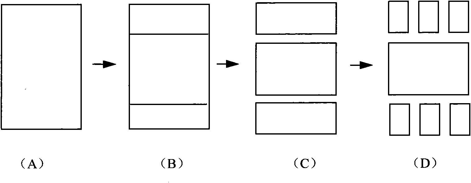
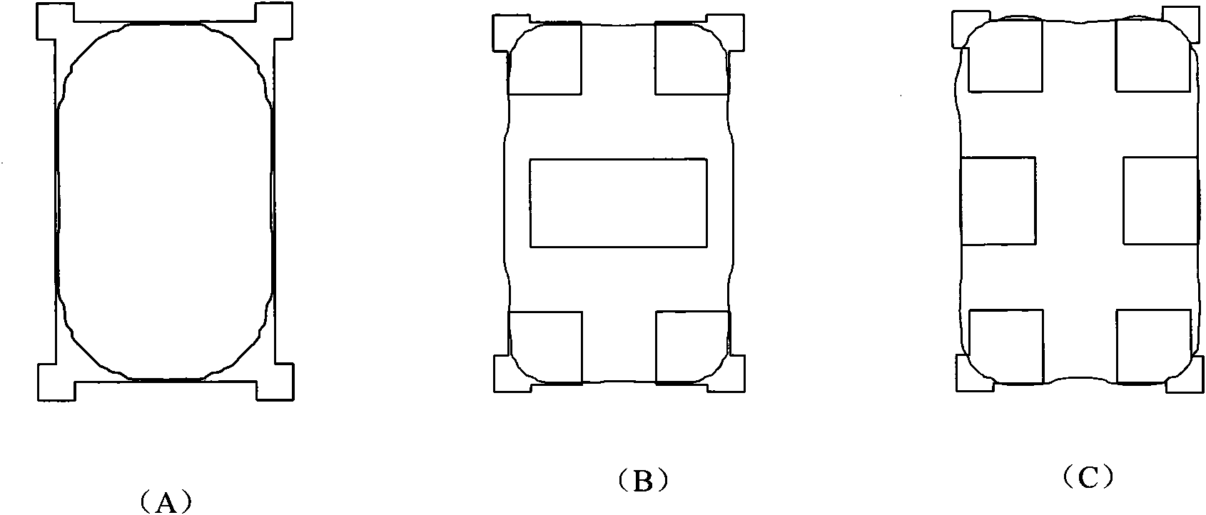
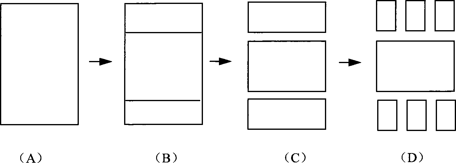
[0019] The present invention provides an optical proximity correction method for improving the fidelity of Si / Ge emitter window patterns, mainly using a series of small hole patterns to form a Si / Ge emitter window layout, and using smaller rectangles to generate corner rounding (corner rounding) The smaller the radius of curvature, the optical proximity effect principle, and the principle that the image cannot be imaged if the pitch is too small, the larger rectangle is split into small holes, the corner rounding is smaller after exposure, and the graphics are closer to the layout, while the middle After exposure, the separated area will have insufficient resolution, and the side lobe (side lobe, side lobe) effect will occur on the edge of the small hole when the hole is overexposed, resulting in the principle of pattern adhesion, so that it wi...


PUM


Abstract

The invention discloses a method for improving the fidelity of a Si / Ge emitter window graph, which comprises the following steps of: 1, designing a Si / Ge emitter window layout, namely (1) cutting a rectangular graph into three parts along a long axis direction in a central symmetry mode, allowing two end parts to have the same size, and allowing the rest part to be a middle part; (2) setting rational intervals between each of the two cut end parts and the middle part; (3) cutting the two end parts into a plurality of structures with holes at certain intervals; and (4) treating the middle part, namely splitting the middle part into a plurality of sets with graphs at certain intervals, or maintaining a whole rectangular structure without splitting; and 2, performing optical proximity correction by adopting the Si / Ge emitter window layout designed by the step 1, and forming a graph approximate to a square by utilizing a principle that a side lobe is generated when a hole of the layout is overexposed.

Description

technical field [0001] The invention belongs to the field of manufacturing technology of Si / Ge devices in semiconductor manufacturing, specifically relates to an optical proximity correction method in the photolithography process of Si / Ge devices, in particular to a method for improving the fidelity of Si / Ge emitter window graphics. Background technique [0002] Based on Si / Ge (Si / Ge refers to Si x Ge 1-x The semiconductor device of the alloy) compound uses the characteristics that the Si / Ge energy band gap is smaller than that of Si and is compatible with the Si integrated circuit process. It is suitable for manufacturing semiconductor devices with high integration, high speed and easy compatibility with Si semiconductor devices. It is widely used Used in high-speed communication field. [0003] In Si / Ge devices, Si / Ge is generally used as the base region, polysilicon is used as the emitter, and the doped substrate is used as the collector. The shape of the emitter window...

Claims


Application Information

Patent Timeline
Patent Type & Authority Applications(China)
IPC IPC(8): G03F1/14G03F1/36
Inventor 王雷
Owner SHANGHAI HUAHONG GRACE SEMICON MFG CORP
Why Eureka
Try Eureka