Connector assembly of solar photovoltaic cell junction box
A technology for photovoltaic cells and connectors, which is applied in the field of improvement of the internal connector structure of photovoltaic cell junction boxes, and can solve problems such as ineffective transmission of solar panel current, complicated production and installation process, and increased production costs of junction boxes. Save equipment and human resources, improve power utilization, and reduce current resistance
- Summary
- Abstract
- Description
- Claims
- Application Information
AI Technical Summary
Problems solved by technology
Method used
Image
Examples
Embodiment 1
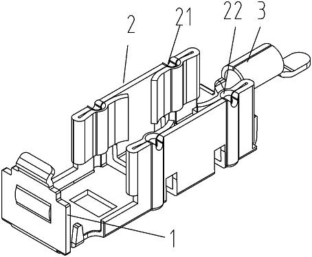
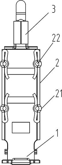
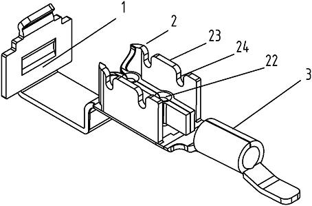
[0023] Such as figure 1 , 2 Shown is the connector of the solar photovoltaic cell junction box, which has a diode socket 2, a cable connection port 3 integrated with the diode socket and a return bar connection port 1, and the diode socket 2 is located between the cable connection port 3 and the diode socket. Between the backflow bar connection ports 1, the diode socket 2 includes a side plate 23 and a diode socket 22, the diode socket 22 is located between the two side plates 23, and the diode socket 22 has two A hollow cylinder formed by bending semicircular concave copper sheets relative to each other. The diameter of the inner hole of the hollow cylinder is slightly smaller than the diode pin connected to it, and the side plate corresponds to the diode socket 22 The position is provided with groove 24, and the effect of groove is to facilitate the insertion of diode and socket 22.
Embodiment 2
[0025] Such as image 3 , 4 Another embodiment of the connector of the solar photovoltaic cell junction box shown has a diode socket frame 2 and a cable connection port 3 integrated with the diode socket frame and a return bar connection port 1, and the diode socket frame 2 resides in Between the cable connection port 3 and the return bar connection port 1, there is a diode socket 22 in the diode socket frame, and the diode socket 22 is located on two sides of the diode socket frame, and has two semicircular concave surfaces. It is a hollow cylinder formed by relatively turning copper sheets. The diameter of the inner hole of the hollow cylinder is slightly smaller than that of the diode pin connected thereto. The diode socket 22 is provided with a notch 21 . The connector of the present invention is stamped by a progressive die.
PUM
 Abstract
Description
Claims
Application Information
 - R&D
- Intellectual Property
- Life Sciences
- Materials
- Tech Scout
- Unparalleled Data Quality
- Higher Quality Content
- 60% Fewer Hallucinations
Browse by: Latest US Patents, China's latest patents, Technical Efficacy Thesaurus, Application Domain, Technology Topic, Popular Technical Reports.
© 2025 PatSnap. All rights reserved.Legal|Privacy policy|Modern Slavery Act Transparency Statement|Sitemap|About US| Contact US: help@patsnap.com


