Manufacturing method of thin film transistor and transistor manufactured by method
A technology of thin film transistors and manufacturing methods, applied in the direction of transistors, semiconductor/solid-state device manufacturing, electrical components, etc., can solve the problems of complicated process, high production cost, and complicated production process of thin film transistors, and achieve small electrode area and simplified manufacturing process , the effect of large numerical aperture
- Summary
- Abstract
- Description
- Claims
- Application Information
AI Technical Summary
Problems solved by technology
Method used
Image
Examples
Embodiment 1
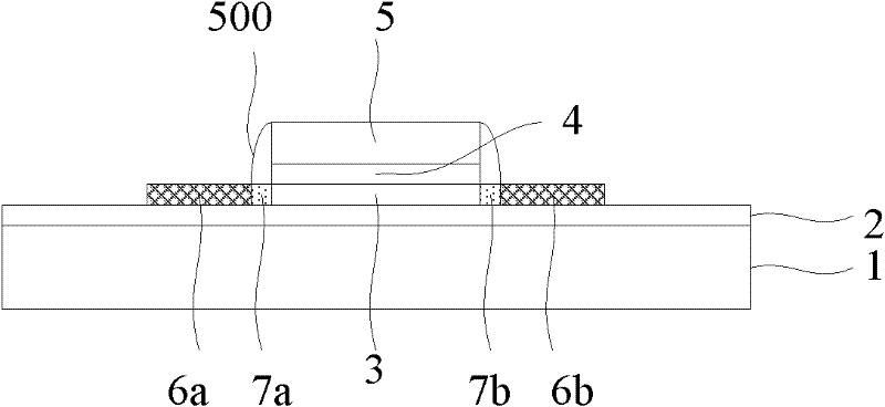
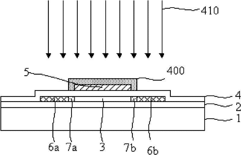
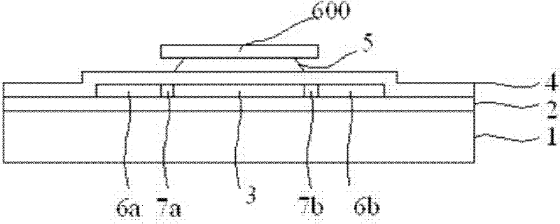
[0028] refer to Figure 4A to Figure 4D , the manufacturing method of the thin film transistor of the present embodiment comprises the following steps:
[0029] (1) Reference Figure 4A , on the glass substrate, quartz or other substrates 1, the surface covering layer 2 and the intrinsic a-Si layer are continuously deposited by PECVD method (the intrinsic a-Si layer is the original state of the polysilicon island active layer 300, only shown in the figure The polysilicon island active layer 300 is shown, and the intrinsic a-Si layer is not shown), wherein the surface covering layer 2 can prevent substrate impurities such as metal ions from diffusing and penetrating into the silicon active layer, which can be made of a single layer of silicon nitride ( SiNx), silicon oxide (SiO 2 ) made or has a double-layer structure, the optimized surface covering layer 2 adopts thick silica. The thickness of the a-Si layer is optimized for
[0030] (2) a-Si layer dehydrogenation
...
Embodiment 2
[0040] The auxiliary layer 910 is formed on the gate conductive layer 510 according to the method of the first embodiment, wherein the auxiliary layer 910 and the gate insulating layer 4 use the same film material and the same manufacturing process. The thickness of the auxiliary layer 910 determines the dopant dose of the lightly doped region, and its thickness is between between. A better example uses silicon nitride as the gate insulating layer. At this time, the auxiliary layer is also silicon nitride. The way to form silicon nitride is to use PECVD process, the reaction gas is SiH4 / NH3, and the optimized auxiliary layer thickness is
[0041] After the LDD formation layer 9 is formed according to the method of Embodiment 1, the photoresist is not removed, and the gate conductive layer 510 is over-etched by a wet method to form the gate 5. The width of the gate is smaller than the width of the photoresist pattern, and the optimized photoresist The width of the pattern i...
Embodiment 3
[0044] A manufacturing method of a thin film transistor according to another embodiment includes the following steps.
[0045] The auxiliary layer 910 is formed on the gate conductive layer 510 according to the method of the first embodiment, wherein the auxiliary layer 910 and the gate insulating layer 4 adopt the same film material and the same manufacturing process. The thickness of the auxiliary layer 910 determines the dopant dose of the lightly doped region, and its thickness is between between. A better example uses silicon nitride as the gate insulating layer. At this time, the auxiliary layer is also silicon nitride. The method of forming silicon nitride is PECVD process, and the reaction gas is SiH4 / NH3. The optimized auxiliary layer thickness and gate insulating layer The same thickness, both
[0046] After the LDD formation layer 9 is formed according to the method of Embodiment 1, the photoresist is not removed, and the gate conductive layer 510 is over-etche...
PUM
 Abstract
Description
Claims
Application Information
 - R&D
- Intellectual Property
- Life Sciences
- Materials
- Tech Scout
- Unparalleled Data Quality
- Higher Quality Content
- 60% Fewer Hallucinations
Browse by: Latest US Patents, China's latest patents, Technical Efficacy Thesaurus, Application Domain, Technology Topic, Popular Technical Reports.
© 2025 PatSnap. All rights reserved.Legal|Privacy policy|Modern Slavery Act Transparency Statement|Sitemap|About US| Contact US: help@patsnap.com


