Semiconductor device and manufacturing method thereof
A manufacturing method, semiconductor technology, applied in semiconductor/solid-state device manufacturing, semiconductor devices, electrical components, etc.
- Summary
- Abstract
- Description
- Claims
- Application Information
AI Technical Summary
Problems solved by technology
Method used
Image

Examples
Embodiment Construction
[0039] Hereinafter, each embodiment is described in detail and examples accompanied by accompanying drawings are used as a reference basis of the present invention. In the drawings or descriptions in the specification, the same reference numerals are used for similar or identical parts. And in the drawings, the shapes or thicknesses of the embodiments may be enlarged, and marked for simplicity or convenience. Furthermore, the parts of each element in the drawings will be described separately. It should be noted that the elements not shown or described in the drawings are forms known to those of ordinary skill in the art. In addition, specific embodiments only The specific mode used for disclosing the present invention is not intended to limit the present invention.
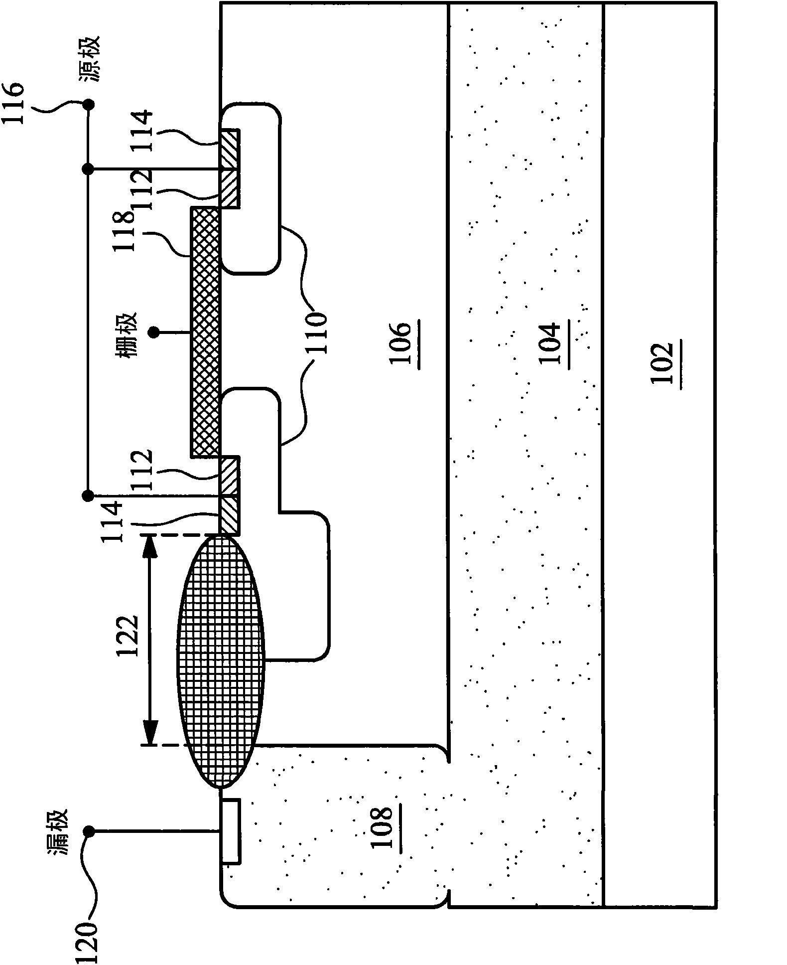
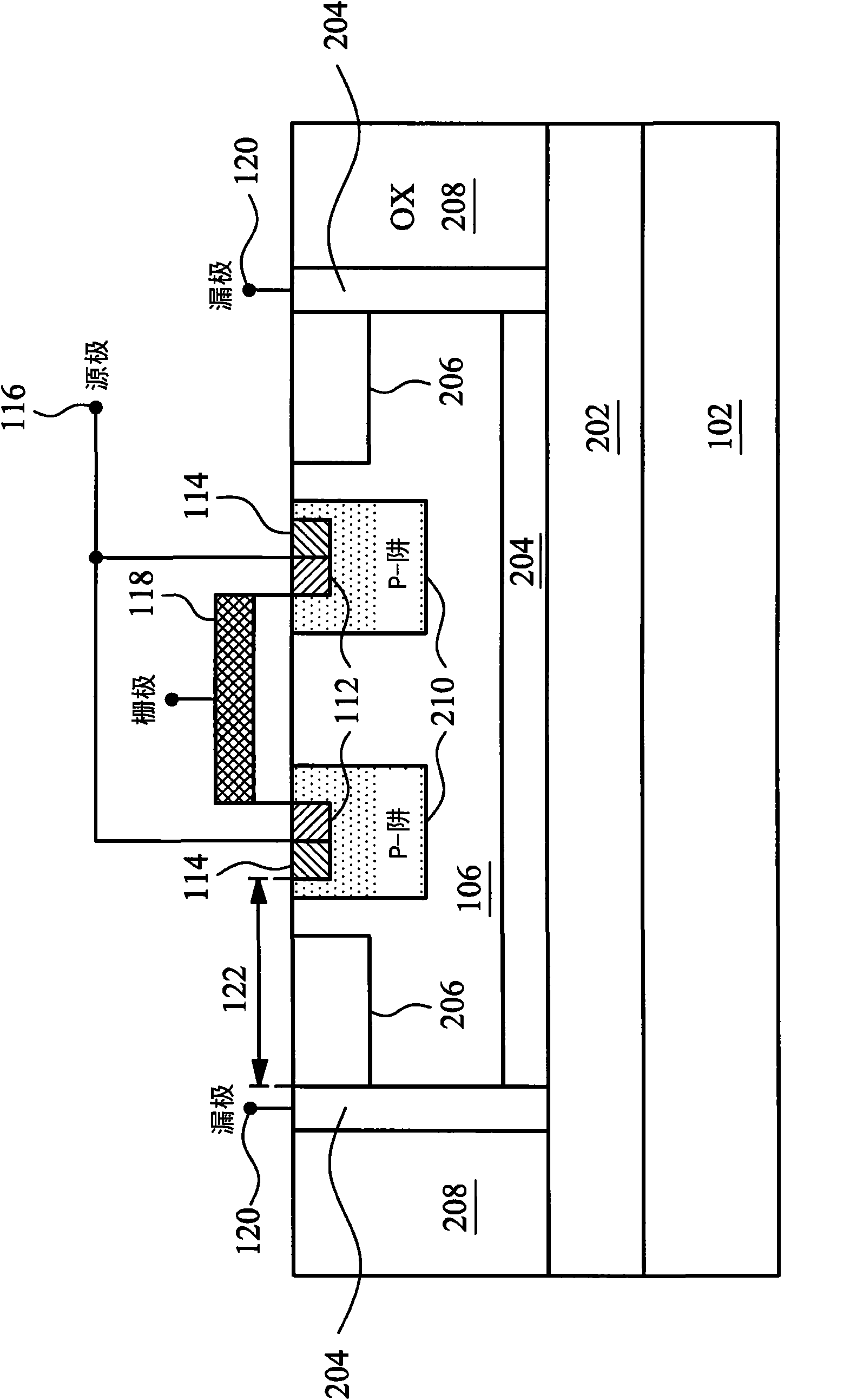
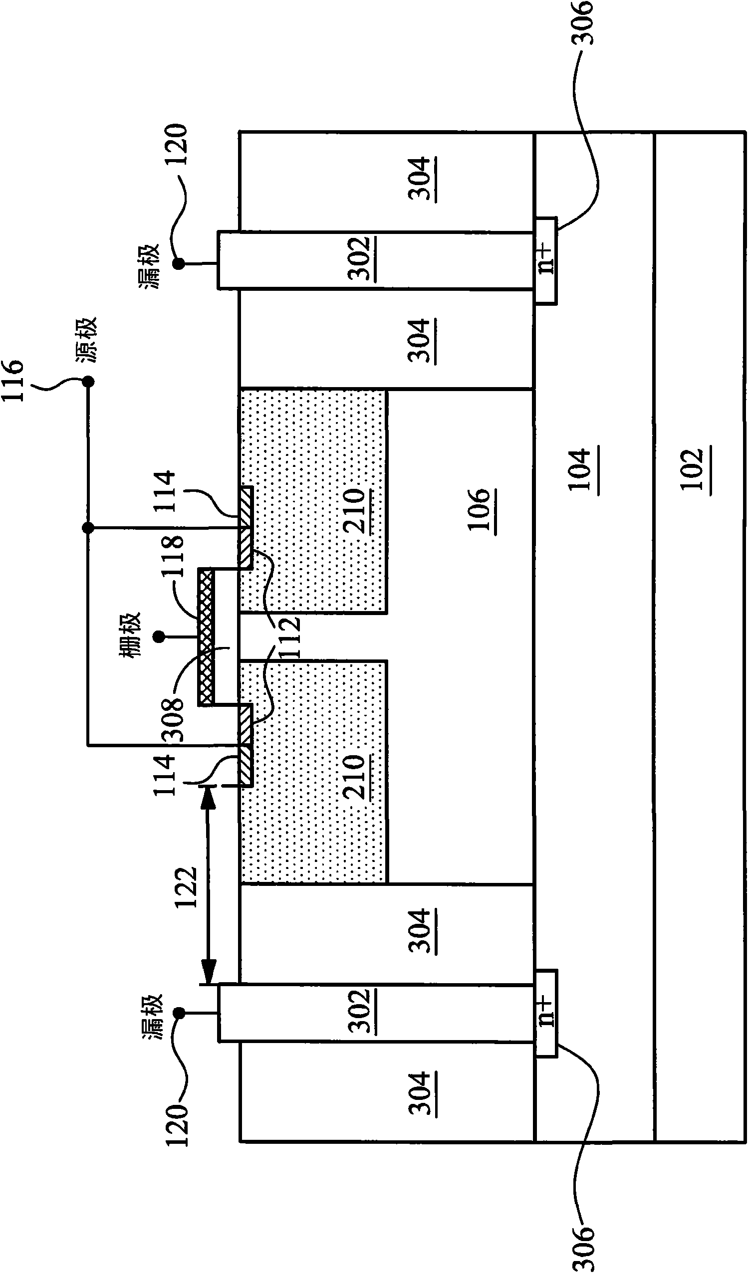
[0040] Embodiments of the present invention provide a metal-oxide-semiconductor (MOS) device structure for high breakdown voltage (BV) and low turn-on resistance R DS on high voltage applications. The embodimen...
PUM
 Abstract
Description
Claims
Application Information
 - R&D
- Intellectual Property
- Life Sciences
- Materials
- Tech Scout
- Unparalleled Data Quality
- Higher Quality Content
- 60% Fewer Hallucinations
Browse by: Latest US Patents, China's latest patents, Technical Efficacy Thesaurus, Application Domain, Technology Topic, Popular Technical Reports.
© 2025 PatSnap. All rights reserved.Legal|Privacy policy|Modern Slavery Act Transparency Statement|Sitemap|About US| Contact US: help@patsnap.com