Ferromagnetic/anti-ferromagnetic multilayer film pinning material and preparation method thereof
An antiferromagnetic layer, antiferromagnetic technology, applied in the application of magnetic film to substrate, multi-layer film of spin exchange coupling, magnetic layer, etc. Excellent binding performance, stable ferromagnetic/antiferromagnetic exchange bias system, and strong practicability
- Summary
- Abstract
- Description
- Claims
- Application Information
AI Technical Summary
Problems solved by technology
Method used
Image


Examples
Embodiment 1
[0044] Embodiment 1: see attached figure 1 .
[0045] A ferromagnetic / antiferromagnetic multilayer film pinning material (magnetic multilayer film system), consisting of substrate 1, buffer layer 2, ferromagnetic layer I 3, antiferromagnetic layer 4, ferromagnetic layer II 5 Composed of protective layer 6;
[0046] Each layer material and parameter are: 1-substrate Si, 2-buffer layer Ta (thickness is 10nm), 3-ferromagnetic layer I SmCo (thickness is 50nm), 4-antiferromagnetic layer FeMn or IrMn (thickness is 10nm ), 5-ferromagnetic layer II NiFe (thickness is 15nm), and 6-protective layer Ta (thickness is 5nm); the thickness or composition of each layer is the value before vacuum deposition or annealing; the vacuum annealing temperature is 550 ° C , keep warm for 0.5 hours, and the vacuum degree is better than 10 -4 Pa.
Embodiment 2
[0047] Embodiment 2: see attached figure 1 .
[0048]A kind of ferromagnetic / antiferromagnetic multilayer film pinning material (magnetic multilayer film system), by: substrate 1, buffer layer 2, ferromagnetic layer 13, antiferromagnetic layer are plated on substrate 1 successively 4. Composition of ferromagnetic layer II 5 and protective layer 6;
[0049] Each layer material and parameter are: 1-substrate Si, 2-buffer layer Ta (thickness is 10nm), 3-ferromagnetic layer I FePt (thickness is 50nm), 4-antiferromagnetic layer FeMn or IrMn (thickness is 10nm ), 5-ferromagnetic layer II NiFe (thickness is 15nm), and 6-protective layer Ta (thickness is 5nm); above-mentioned each layer thickness or composition is the value before vacuum deposition sample or annealing; Vacuum annealing temperature is 600 ℃, keep warm for 1 hour, and the vacuum degree is better than 10 -4 Pa.
Embodiment 3
[0050] Embodiment 3: see attached figure 2 .
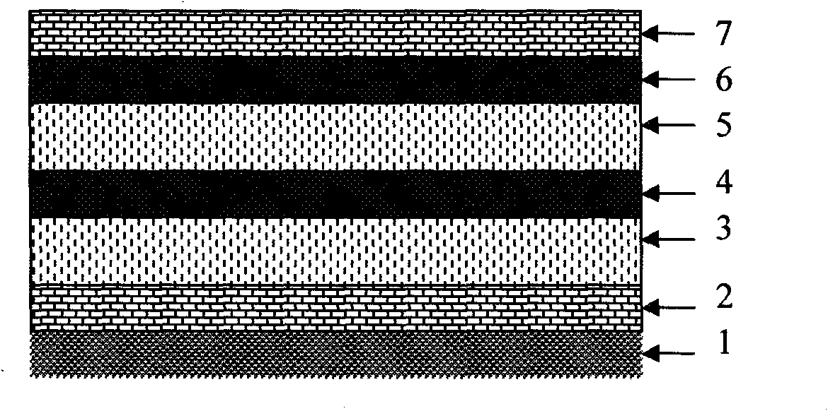
[0051] A ferromagnetic / antiferromagnetic multilayer film pinning material (magnetic multilayer film system), consisting of: a substrate 1, on which a buffer layer 2, a first ferromagnetic layer 3, and a first antiferromagnetic layer are sequentially plated on the substrate 1. The ferromagnetic layer 4, the second ferromagnetic layer 5, the second antiferromagnetic layer 6 and the protective layer 7 are composed.
[0052] Each layer material and parameter are: 1-substrate Si, 2-buffer layer Ta (thickness is 5nm), 3-the first ferromagnetic layer NiFe (thickness is 15nm), 4-the first antiferromagnetic layer FeMn (thickness is 5nm). 2.5nm), 5-second ferromagnetic layer NiFe (thickness is 10nm), 6-second antiferromagnetic layer FeMn (thickness is 10nm) and 7-protective layer Ta (thickness is 5nm); above-mentioned each layer thickness or composition All are the values when the samples are vacuum deposited; attached image 3 Be the...
PUM
| Property | Measurement | Unit |
|---|---|---|
| Thickness | aaaaa | aaaaa |
| Thickness | aaaaa | aaaaa |
| Thickness | aaaaa | aaaaa |
Abstract
Description
Claims
Application Information
 - R&D
- Intellectual Property
- Life Sciences
- Materials
- Tech Scout
- Unparalleled Data Quality
- Higher Quality Content
- 60% Fewer Hallucinations
Browse by: Latest US Patents, China's latest patents, Technical Efficacy Thesaurus, Application Domain, Technology Topic, Popular Technical Reports.
© 2025 PatSnap. All rights reserved.Legal|Privacy policy|Modern Slavery Act Transparency Statement|Sitemap|About US| Contact US: help@patsnap.com