Bionic micro/nano structure preparing method
A technology of micro-nano structure and nano-structure, applied in the field of bionic micro-nano structure preparation, can solve the problems of difficulty in preparing a complete structure, expensive equipment, slow processing speed, etc., and achieve the effect of promoting preparation and application and low cost
- Summary
- Abstract
- Description
- Claims
- Application Information
AI Technical Summary
Problems solved by technology
Method used
Image
Examples
Embodiment 1
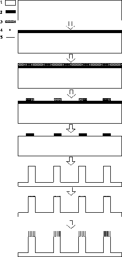
[0020] Example 1. Preparation of micro-nano structure on the surface of imitating butterfly phosphor wings.
[0021] The embodiment 1 of the present invention is used to prepare the micro-nano structure on the surface of imitating butterfly phosphor wings. figure 1 . A layer of SiO is thermally grown on the surface of Si substrate 2 , Using photolithography technology to transfer the micro-scale pattern on the mask to the spin-coated photoresist surface, and put the exposed film into the developer to dissolve the unnecessary photoresist to obtain the required etching The pattern with resist protection is further used RIE dry etching to transfer the pattern to SiO 2 . Using ICP deep etching, a periodic or quasi-periodic micro-scale structure is obtained, and the sidewall must retain sufficient corrugation depth during ICP etching. Then, an electron beam evaporation process is used to evaporate the nano-structure growth seed obliquely, and then grow the nano-structure directionall...
Embodiment 2
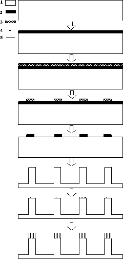
[0030] Example 2. Preparation of the micro-nano structure on the surface of the imitation gecko foot.
[0031] Example 2 of the present invention is used to prepare the micro-nano structure on the surface of the imitation gecko foot. figure 2 . A layer of SiO is thermally grown on the surface of Si substrate 2 , Using photolithography technology to transfer the micro-scale pattern on the mask to the spin-coated photoresist surface, and put the exposed film into the developer to dissolve the unnecessary photoresist to obtain the required etching The pattern with resist protection is further used RIE dry etching to transfer the pattern to SiO 2 . Using ICP deep etching, micro-scale structures with periodic / quasi-periodic distribution are obtained. Then, the electron beam evaporation process is used to evaporate the nanostructure growth seeds on the top of the microscale structure, and then the nanostructures are grown directionally to obtain the micro-nano structure on the surfa...
PUM
 Abstract
Description
Claims
Application Information
 - R&D
- Intellectual Property
- Life Sciences
- Materials
- Tech Scout
- Unparalleled Data Quality
- Higher Quality Content
- 60% Fewer Hallucinations
Browse by: Latest US Patents, China's latest patents, Technical Efficacy Thesaurus, Application Domain, Technology Topic, Popular Technical Reports.
© 2025 PatSnap. All rights reserved.Legal|Privacy policy|Modern Slavery Act Transparency Statement|Sitemap|About US| Contact US: help@patsnap.com


