Drift step recovery diode and preparation method thereof

A recovery diode, N-type technology, applied in semiconductor/solid-state device manufacturing, electrical components, electric solid-state devices, etc., can solve the problems of DSRD devices such as large pre-pulse energy, small voltage pulse, and large pulse front, and shorten the N-base area, the pre-pulse energy is small, and the effect of reducing forward loss

Inactive Publication Date: 2010-07-14
THE 13TH RES INST OF CHINA ELECTRONICS TECH GRP CORP
View PDF0 Cites 7 Cited by
  • Summary
  • Abstract
  • Description
  • Claims
  • Application Information

AI Technical Summary

Problems solved by technology

[0005] The technical problem to be solved in the present invention is to change the internal structure of the DSRD device to solve the problems of large pulse front, small voltage pulse on the load, and large pre-pulse energy loss on the DSRD device

Method used


Image

  • Drift step recovery diode and preparation method thereof
  • Drift step recovery diode and preparation method thereof
  • Drift step recovery diode and preparation method thereof

Examples


Embodiment Construction

[0014] The present invention will be described in further detail below in conjunction with the accompanying drawings.

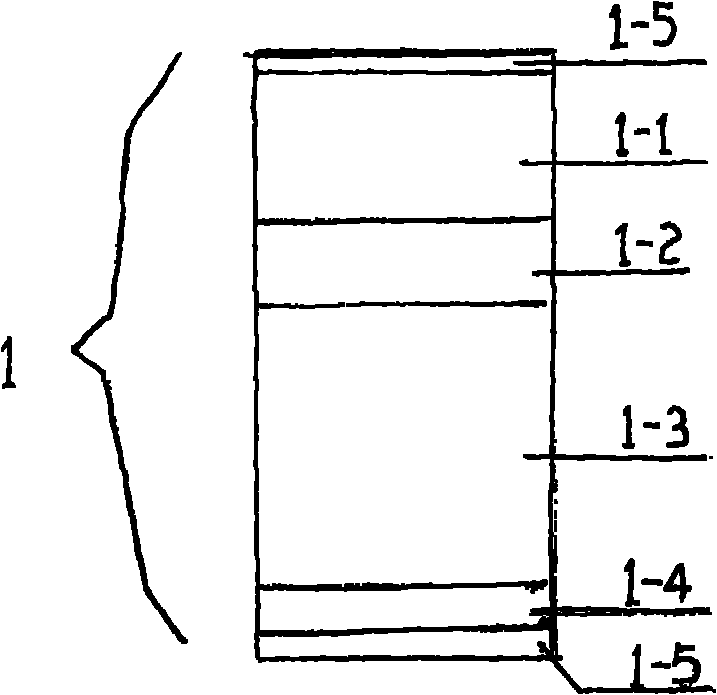
[0015] see figure 1 , the drift step recovery diode DSRD provided by the present invention, its base is an N-type substrate 1, and phosphorus-doped N is formed inside the N-type substrate 1 by doping + Region 1-1, aluminum-doped P region 1-3, boron-doped P + Zones 1-4; where N + Zone 1-1 with P + Regions 1-4 are located on both sides of the N-type substrate 1, and the P + Zone 1-4 is adjacent to P zone 1-3, P zone 1-3 is adjacent to N + Zone 1-1 is isolated by N Zone 1-2, where P + The total junction depth of regions 1-4 and P regions 1-3 is 100 μm˜130 μm. above N + The junction depth of the region 1-1 is 50 μm to 120 μm. In this embodiment, the N-type substrate 1 is preferably a silicon substrate.

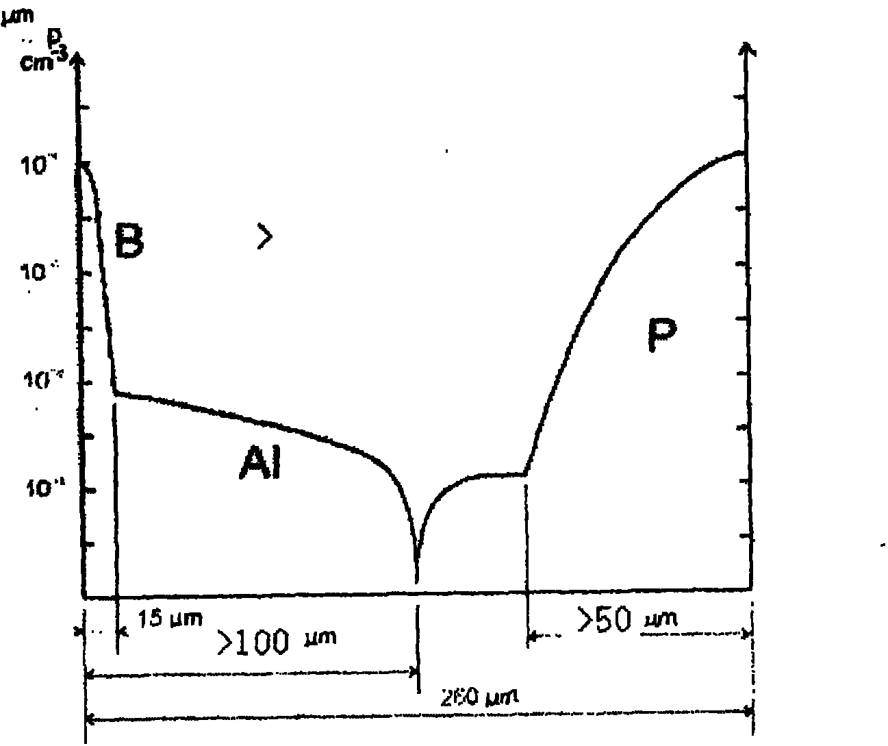
[0016] see figure 2 Shown is the doping curve for a DSRD with a 1 ns pulse front at a voltage of 1 KV. The initial resistivity of the material of the...


PUM

PropertyMeasurementUnit
Knot deepaaaaaaaaaa
Thicknessaaaaaaaaaa
Resistivityaaaaaaaaaa

Abstract

The invention provides a drift step recovery diode used as a switch in a nanosecond pulse source device and a preparation method thereof. A matrix is an N-type substrate (1), and a phosphorus-doped N+ region (1-1), an aluminum-doped P region (1-3) and a boron-doped P+ region (1-4) are arranged in the N-type substrate (1) through doping, wherein the N+ region (1-1) and the P+ region (1-4) are positioned on the two sides of the N-type substrate (1); the P+ region (1-4) is adjacent to the P region (1-3); and the P region (1-3) is separated from the N+ region (1-1) through an N region (1-2). The drift step recovery diode is characterized in that the total junction depth of the P+ region (1-4) and the P region (1-3) is 100-130 mu m. By changing the internal structure of a drift step recovery diode (DSRD) device, the problems such as large pulse front edge, small voltage pulse on load and large prepulse energy consumption on the DSRD device are solved so as to improve the cut-off velocity of DSRD switches.

Description

technical field [0001] The invention relates to a semiconductor switch diode, in particular to a drift step recovery diode (DSRD) used as a switch in a nanosecond pulse source device and a preparation method thereof. Background technique [0002] In the UWB pulse source, the key electronic component for generating UWB pulses from picoseconds to nanoseconds is the switch. When generating nanosecond-level high-voltage pulses, traditional devices (such as plasma circuit breakers, injection thyratrons and blasting wires, etc.) have short lifespans, poor impact resistance and cannot be reused. Traditional semiconductor devices, such as the fastest current cut-off time with a dedicated field effect transistor, need 10 ns and the system is very complicated and expensive. The duration of the current cut-off process of traditional high-power high-voltage semiconductor diodes is on the order of microseconds, which is much higher than that on the order of nanoseconds. Can not meet th...

Claims


Application Information

Patent Timeline
IPC IPC(8): H01L29/861H01L29/06H01L27/08H01L21/329H01L21/77
Inventor 刘忠山杨勇崔占东
Owner THE 13TH RES INST OF CHINA ELECTRONICS TECH GRP CORP
Why Eureka
Try Eureka