
Graphene/silicon carbide Schottky junction based photovoltaic cell and preparation method thereof

A photovoltaic cell and Schottky junction technology, applied in photovoltaic power generation, circuits, electrical components, etc., can solve the problems of inability to synthesize the macroscopic structure of photovoltaic performance carbon nanotubes, inability to precisely control the chirality of carbon tubes, and large voids in the network structure. , to achieve the effect of suitable for large-scale application, excellent light transmission and conductivity, and low cost

Active Publication Date: 2010-07-07
TSINGHUA UNIV
View PDF1 Cites 61 Cited by
  • Summary
  • Abstract
  • Description
  • Claims
  • Application Information

AI Technical Summary

Problems solved by technology

However, for carbon nanotubes, the limitations of existing preparation technologies have become an important obstacle to their industrialization. It is still impossible to precisely control the chirality of carbon nanotubes, and it is impossible to synthesize macroscopic carbon nanotubes with controllable photovoltaic properties. structure
Carbon nanotubes also have disadvantages as thin-film electrode materials in solar cells, such as the need for post-treatment processes such as purification, and the network structure formed by the tube bundles has large gaps, large surface roughness, and a theoretical upper limit for electrical conductivity (L.F.C.Pereira, et al. .Appl.Phys.Lett.2009, 95, 123106), there is no room for further improvement

Method used


Image

  • Graphene/silicon carbide Schottky junction based photovoltaic cell and preparation method thereof
  • Graphene/silicon carbide Schottky junction based photovoltaic cell and preparation method thereof
  • Graphene/silicon carbide Schottky junction based photovoltaic cell and preparation method thereof

Examples


Embodiment Construction

[0019] The structural principle and working principle of the present invention will be described in detail below in conjunction with the accompanying drawings.

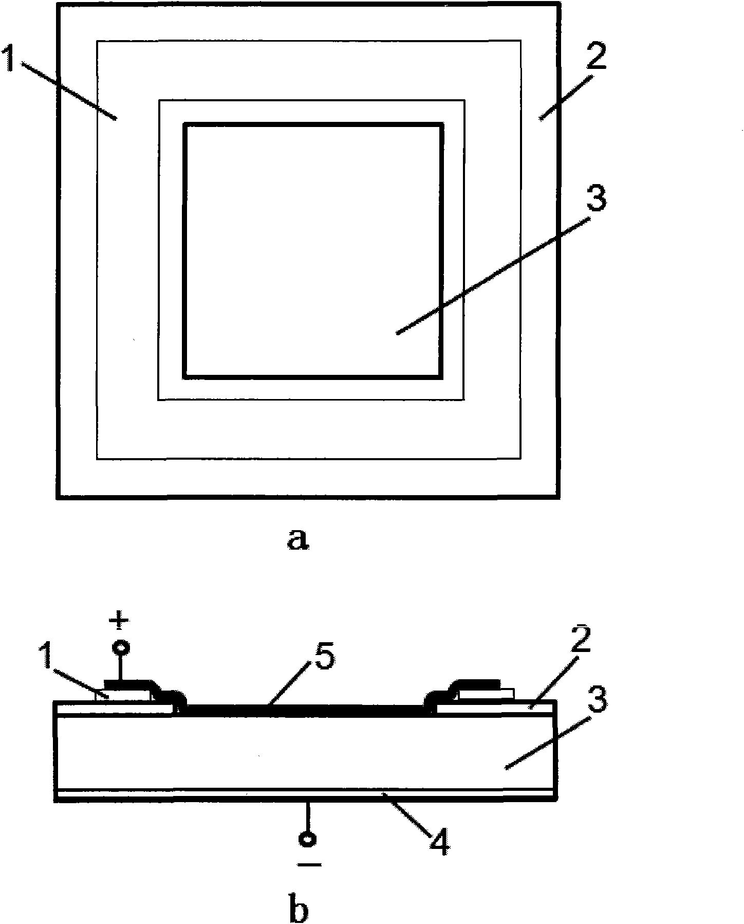
[0020] refer to figure 1 , a kind of photovoltaic cell based on graphene / silicon Schottky junction, is characterized in that, comprises titanium palladium silver TiPdAg back electrode 4, is placed on the titanium palladium silver TiPdAg back electrode 4 with n-type monocrystalline silicon n-Si 3, Silicon dioxide SiO is placed on the n-type single crystal silicon wafer n-Si 3 2 Layer 2, silicon dioxide SiO 2 There is a through hole in the middle of layer 2, silicon dioxide SiO 2 A ring-shaped gold film 1 is placed on the layer 2, the inner hole of the gold film 1, the SiO 2 The through hole in the middle of the layer 2 and the upper surface of the n-type single crystal silicon chip n-Si 3 form a step hole, and one end of the titanium palladium silver TiPdAg back electrode 4 leads out a wire, and a graphene film 5 is...


PUM


Abstract

The invention provides a graphene / silicon carbide Schottky junction based photovoltaic cell and a preparation method thereof. The method comprises the following steps: placing a TiPdAg back electrode, an n-type monocrystalline silicon piece n-Si, an annular SiO2 layer and an annular gold film from bottom to top in a laminating mode, and forming stepped holes by an inner hole of the gold film, a through hole in the middle of the SiO2 layer and the upper surface of the n-type monocrystalline silicon piece n-Si; tiling the graphene or organic suspension of the graphene on the surface of the stepped holes by methods of directly transferring, spin coating, spraying, dipping and filtering, and leading the dried graphene film to be closely combined with the n-Si on a substrate electrode; and taking a lead wire extracted from one end of the graphene film as an anode of the photovoltaic cell, and taking a lead wire extracted from one end of the TiPdAg back electrode as a cathode of the photovoltaic cell. The photovoltaic cell reduces the utilization ratio of silicon, has simple assembly process and low cost, and is applicable to scale application.

Description

technical field [0001] The invention relates to the field of nano-carbon material devices and applications, in particular to a graphene / silicon Schottky junction-based photovoltaic cell and a preparation method thereof. Background technique [0002] In the field of solar energy utilization, silicon is the most commercially valuable photovoltaic material. However, high energy consumption, noise, waste, and pollution are some of the major problems it faces. In recent years, its negative effects have become increasingly prominent, and related technologies and industries have begun to appear bottleneck effects. At present, people are trying their best to find new materials that can replace silicon, and develop new technologies to reduce the usage rate of silicon and make photovoltaic cells with higher efficiency and more environmental protection. [0003] In the process of searching for new materials and new technologies, nanomaterials and nanotechnology are one of the current...

Claims


Application Information

Patent Timeline
IPC IPC(8): H01L31/042H01L31/0224H01L31/18
CPCY02E10/50H01L29/47
Inventor 李昕明朱宏伟王昆林韦进全李春艳贾怡李祯李虓吴德海
Owner TSINGHUA UNIV
Learn More