High-voltage LDMOS device
A high-voltage, device technology, applied in the field of semiconductor integrated circuit structure, can solve the problems of device snapback breakdown, NPN transistor turn-on, hot carrier effect deterioration, etc., to meet the breakdown voltage, reduce electric field strength, high breakdown The effect of voltage
- Summary
- Abstract
- Description
- Claims
- Application Information
AI Technical Summary
Problems solved by technology
Method used
Image
Examples
Embodiment Construction
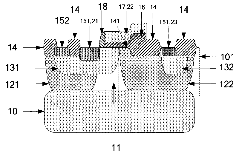
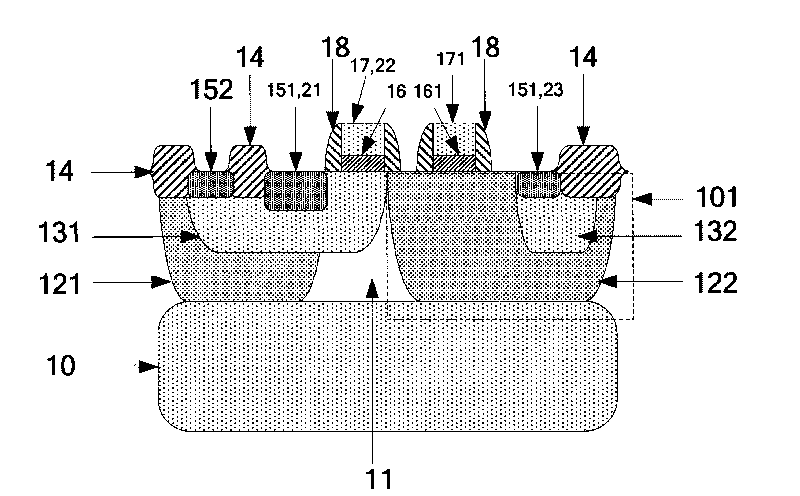
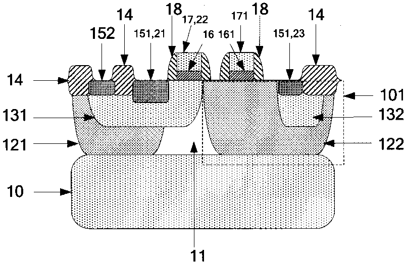
[0012] see figure 2 , the high voltage LDMOS device of the present invention comprises:
[0013] The N-type buried layer 10 is at the bottom of the LDMOS device;
[0014] N-type epitaxial layer 11, on the N-type buried layer 10;
[0015] The N-type epitaxial layer 11 includes horizontally arranged high-voltage P wells 121 and high-voltage N wells 122;
[0016] The low-voltage P well 131 is in the high-voltage P well 121, or in the high-voltage P well 121 and the adjacent N-type epitaxial layer 11;
[0017] A low-voltage N-well 132 within the high-voltage N-well 122;
[0018] The field oxide layer 14 is outside the P-type active region 152 , between the P-type active region 152 and the N-type active region 151 in the low-voltage P-well 131 , and outside the N-type active region 151 in the low-voltage N-well 132 .
[0019] The N-type active region 151 is respectively in the low-voltage P well 131 and the low-voltage N well 132; wherein the N-type active region 151 in the lo...
PUM
 Abstract
Description
Claims
Application Information
 - R&D Engineer
- R&D Manager
- IP Professional
- Industry Leading Data Capabilities
- Powerful AI technology
- Patent DNA Extraction
Browse by: Latest US Patents, China's latest patents, Technical Efficacy Thesaurus, Application Domain, Technology Topic, Popular Technical Reports.
© 2024 PatSnap. All rights reserved.Legal|Privacy policy|Modern Slavery Act Transparency Statement|Sitemap|About US| Contact US: help@patsnap.com


