Bipolar transistor and manufacturing method thereof

A technology for bipolar transistors and manufacturing methods, which is applied in the direction of transistors, semiconductor/solid-state device manufacturing, semiconductor devices, etc., and can solve problems such as insufficient compatibility of bipolar transistors, difficulty in effectively controlling the breakdown voltage of emitters and collectors, etc.

Active Publication Date: 2012-03-07
SEMICON MFG INT (SHANGHAI) CORP
View PDF1 Cites 0 Cited by
  • Summary
  • Abstract
  • Description
  • Claims
  • Application Information

AI Technical Summary

Problems solved by technology

[0004] Traditional bipolar transistors have many disadvantages, such as the breakdown voltage between the emitter and collector is difficult to effectively control, etc.
[0005] In addition, bipolar transistors are not sufficiently compatible with existing MOS transistor manufacturing processes

Method used


Image

  • Bipolar transistor and manufacturing method thereof
  • Bipolar transistor and manufacturing method thereof
  • Bipolar transistor and manufacturing method thereof

Examples


Embodiment 1

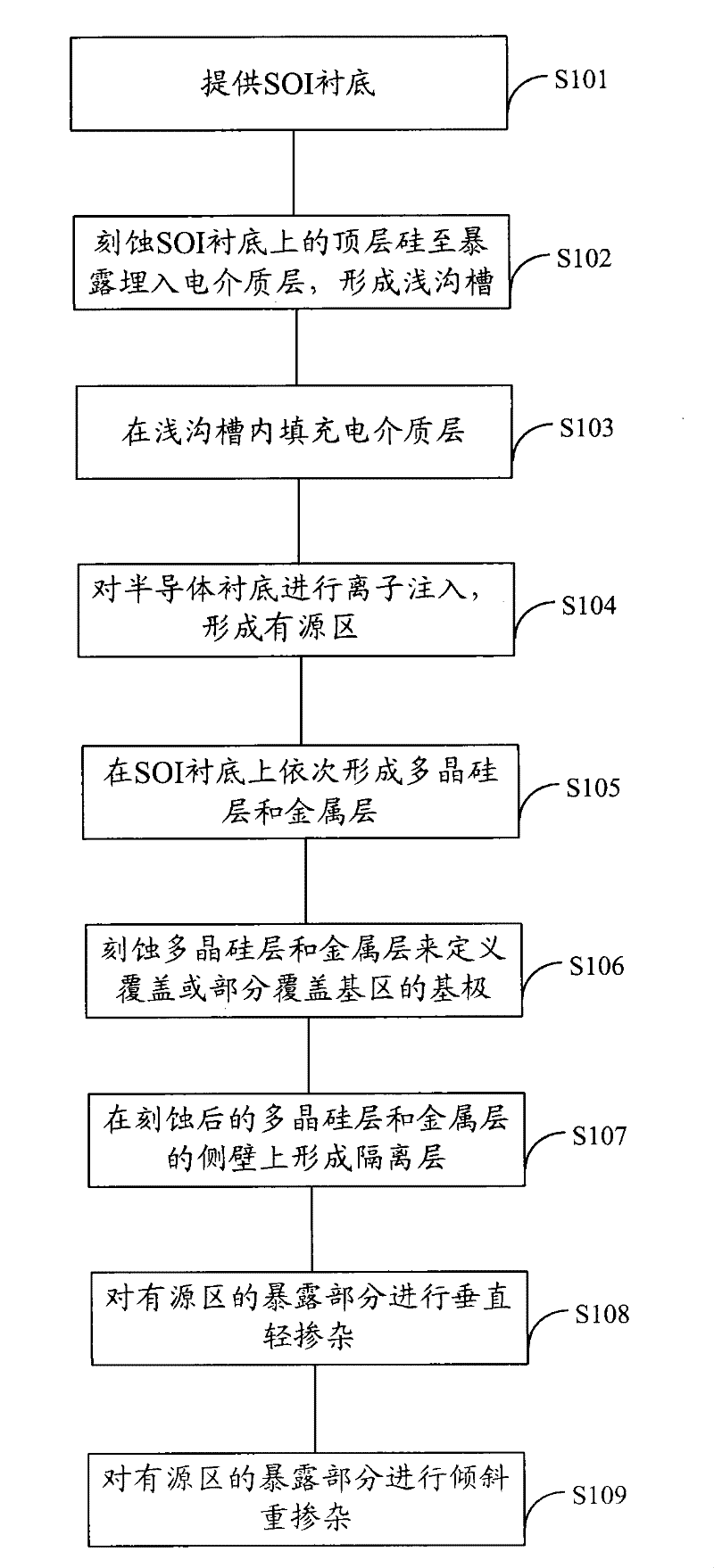
[0028] In the following, a bipolar transistor structure formed on an SOI (Silicon On Insulator, silicon-on-insulator) substrate and its manufacturing method are taken as an example, and the specific implementation manner of the present invention will be described in detail in conjunction with the accompanying drawings.

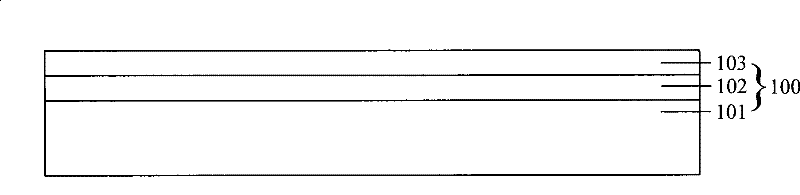
[0029] The SOI substrate has an underlying silicon substrate, a buried dielectric layer, and a first semiconductor material layer on the buried dielectric layer. The material of the first semiconductor material layer includes Si, Ge, SiGe, GaAs, InP, InAs or InGaAs, etc. In Embodiment 1, the material of the first semiconductor material layer is silicon as an example for detailed description.

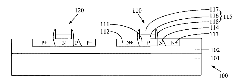
[0030] Such as figure 1 As shown, on the top layer silicon 103 of the SOI substrate 100 (reference image 3 ) is formed with an NPN bipolar transistor 110. The NPN bipolar transistor 110 includes a P-type base region 111 , an N-type emitter region 112 and an N-type col...

Embodiment 2

[0066] In this specific embodiment, a special bipolar transistor structure with a buffer zone formed on an SOI substrate and its manufacturing method are also provided, which will be described below with reference to the accompanying drawings.

[0067] Such as Figure 12 and Figure 13 As shown, the present embodiment provides a bipolar transistor 201 formed on an SOI substrate 220, including a metal base 202 formed of metal and a cylindrical semiconductor material column 203 (refer to Figure 20 ). The semiconductor material pillar 203 is, from one end to the other end, an emitter region 204 , a base region 205 , a buffer region 208 and a collector region 206 of the bipolar transistor 201 in sequence. A through hole 207 is formed in the metal base 202 , and the base region 205 is located in the through hole 207 , that is, the metal base 202 forms a wrap around the base region 205 and exposes the emitter region 204 and the collector region 206 . The length of the base regio...


PUM

PropertyMeasurementUnit
lengthaaaaaaaaaa
thicknessaaaaaaaaaa
thicknessaaaaaaaaaa

Abstract

The invention relates to a bipolar transistor and a manufacturing method thereof. The method for manufacturing the bipolar transistor comprises the following steps of: providing a semiconductor substrate; performing ion implantation on the first semiconductor material layer; etching the first semiconductor material layer and an embedding dielectric layer to form a semiconductor material pillar and a dielectric support pillar; removing the middle segment of the dielectric support pillar; depositing a metal layer on the substrate to at least embed the semiconductor material pillar; etching the metal layer to form a metal base electrode; performing vertical light doping on the exposed part at both ends of the semiconductor material pillar; and performing inclined heavy doping on the exposed part of the semiconductor material pillar. The invention ensures that a heavily doped emission region contacted with the base region and a lightly doped buffer region between the base region and the heavily doped collector region can be formed in one step by firstly performing vertical light doping and then performing inclined heavy doping on the emission region and the collector region so as to control puncture voltage between the emission region and the collector region by controlling the heavy doping angle.

Description

technical field [0001] The invention relates to the manufacturing field of semiconductor devices, in particular to a bipolar transistor and a manufacturing method thereof. Background technique [0002] Bipolar transistors have two basic structures: PNP type and NPN type, which consist of two back-to-back PN junctions. Among the three layers of semiconductors, the middle layer is called the base region (B), and the left and right layers are called the emitter region (E) and the collector region (C). An emitter junction is formed between the emitter region and the base, and a collector junction is formed between the collector region and the base. Transistors can be divided into low-power transistors, medium-power transistors, and high-power transistors according to their power dissipation capabilities. According to the level of working frequency, it can be divided into low frequency tube, high frequency tube and microwave tube. According to the manufacturing process, it can...

Claims


Application Information

Patent Timeline
Patent Type & Authority Patents(China)
IPC IPC(8): H01L29/73H01L29/06H01L21/331
Inventor 肖德元季明华
Owner SEMICON MFG INT (SHANGHAI) CORP
Why Eureka
Try Eureka