Bidirectional large-through-flow low-residual-voltage TVS device

A low residual voltage and flow-through technology, which is applied in the direction of semiconductor devices, semiconductor/solid-state device manufacturing, electrical components, etc., can solve the problems of isolation leakage, increase of TVS junction area, and decrease of product competitiveness, etc., and achieve large surge pass-through Flow capacity, not easy to break through, save area

Pending Publication Date: 2020-10-30
SHANGHAI CHANGYUAN WAYON MICROELECTRONICS
View PDF0 Cites 0 Cited by
  • Summary
  • Abstract
  • Description
  • Claims
  • Application Information

AI Technical Summary

Problems solved by technology

[0003] The traditional way of increasing the surge current capability of TVS is usually to increase the area of ​​the PN junction. However, simply increasing the area will bring a series of problems, mainly including: ①. The increase in the area of ​​TVS devices leads to the use of larger packages , unable to meet the miniaturization requirements of the application side
②. Simply increase the TVS junction area, the cost will rise, and the product competitiveness will decline
③. Reducing VBR can reduce the residual voltage of the device to a certain extent, but the problem is the increase of leakage current
Poor isolation will cause problems such as leakage and low breakdown

Method used


Image

  • Bidirectional large-through-flow low-residual-voltage TVS device
  • Bidirectional large-through-flow low-residual-voltage TVS device
  • Bidirectional large-through-flow low-residual-voltage TVS device

Examples


Embodiment 1

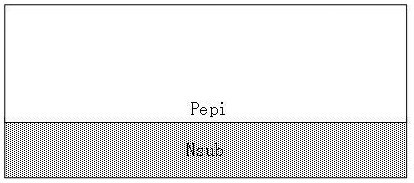
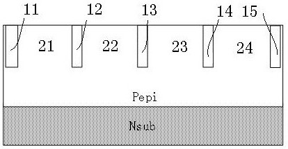
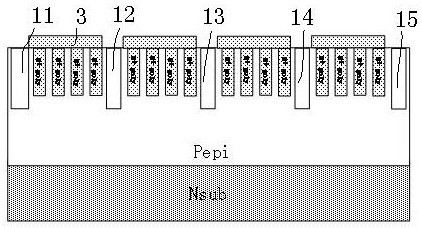
[0040] like Figures 1 to 5 As shown, a bidirectional large flow-through and low residual voltage TVS device forms a P-type epitaxial Pepi on the N+ substrate Nsub, and fills the P-type epitaxial Pepi with low-pressure tetraethoxysilane (LPTEOS) to a depth of 2--5um. Shallow trenches with a width of 1-1.2 μm, trench one 11, trench two 12, trench three 13, trench four 14, and trench five 15 are used as isolation grooves to form isolation areas 1 21, 2 22, and 2 with the same size and spacing. Three 23, isolation area four 24; each isolation area is provided with multiple polys with the same structure, equal spacing, depth of 1-4 μm and filled with N+ poly body 3; deposit a layer of SiO as a contact hole on the surface of N+ poly 2 The dielectric layer 4 retains the lead-out position of the N+ poly body 3 between every two isolation grooves, and deposits the metal layer 5 as the lead-out electrode; wherein, the lead-out electrodes of the isolation region 1 21 and the isolation r...

Embodiment 2

[0059] A TVS device with bidirectional large current flow and low residual voltage, which is similar to Embodiment 1, except that the N+ Poly body is changed to an N+ region, such as Figure 7 Shown:

[0060] Form P-type epitaxy on the N+ substrate, and use LPTEOS to fill shallow grooves with a depth of 2--5um and a width of 1-1.2um on the P-type epitaxy. Trench one 11, trench two 12, trench three 13, trench four 14, Trench 5 15 is used as an isolation groove to form four isolation areas 1 21, 2 22, 3 23, and 4 24 with the same size and spacing; each isolation area is provided with the same structure, equal spacing, and a depth of 1-4μm N+ region 3'; deposit a layer of SiO as a contact hole on the surface of N+ region 3' 2 The dielectric layer 4 retains the lead-out position of the N+ region 3' between every two isolation grooves, and deposits a metal layer 5 as the lead-out electrode; wherein, the lead-out electrodes of the isolation region 1 21 and the isolation region 3 23...


PUM

PropertyMeasurementUnit
widthaaaaaaaaaa
electrical resistivityaaaaaaaaaa

Abstract

The invention discloses a bidirectional large-through-flow low-residual-voltage TVS device. The device comprises a P-type doped epitaxial wafer, an N-type substrate slice, an isolation trench, and anN + polycrystalline poly groove, the novel TVS device provided by the invention is a bidirectional device, the clamping voltage is reduced while the peak current IPP in the breakdown direction is greatly improved, so that the protected device is completely located in a safe region, and different BV breakdown voltages can be realized by adjusting the depth of the isolation trench. By using the isolation trench, the distance between N + poly junctions can be maintained to be 1-1.2 [mu] m; the N + polycrystal poly groove realizes that the effective area of the N + junction can be maximized underthe condition of the same area, the surge capacity of the TVS is greatly improved, and the obtained TVS device has the advantages of high power, small size, high integration level, low cost and the like.

Description

technical field [0001] The invention relates to a TVS device with bidirectional large current flow and low residual voltage and relates to the technical field of semiconductors, in particular to a TVS device with bidirectional large current flow and low residual voltage and a manufacturing method thereof. Background technique [0002] Transient voltage suppressors (TVS) are widely used in various electronic products. With the reduction of circuit operating voltage, the chip size is also decreasing, so higher requirements are put forward for the corresponding TVS protection devices. On the one hand, the area of ​​TVS protection devices is required to be smaller and smaller to match the shrinking main chip size; on the other hand, with the increasing requirements for security and reliability of various mobile terminal equipment, TVS The protection device must not only have a high surge current protection capability, but also have a low clamping voltage. [0003] The tradition...

Claims


Application Information

Patent Timeline
Patent Type & Authority Applications(China)
IPC IPC(8): H01L29/06H01L29/861H01L21/329
CPCH01L29/0649H01L29/0684H01L29/66128H01L29/8611
Inventor 张啸赵德益李亚文赵志方蒋骞苑王允吕海凤霍田佳
Owner SHANGHAI CHANGYUAN WAYON MICROELECTRONICS
Why Eureka
Try Eureka