Single programmable read-only memory and method of manufacture
A manufacturing method and memory technology, which are applied in semiconductor/solid-state device manufacturing, electrical solid-state devices, semiconductor devices, etc., can solve the problems of inconsistent characteristics of memory cells, easy leakage, etc. crash effect
- Summary
- Abstract
- Description
- Claims
- Application Information
AI Technical Summary
Problems solved by technology
Method used
Image

Examples
no. 1 example
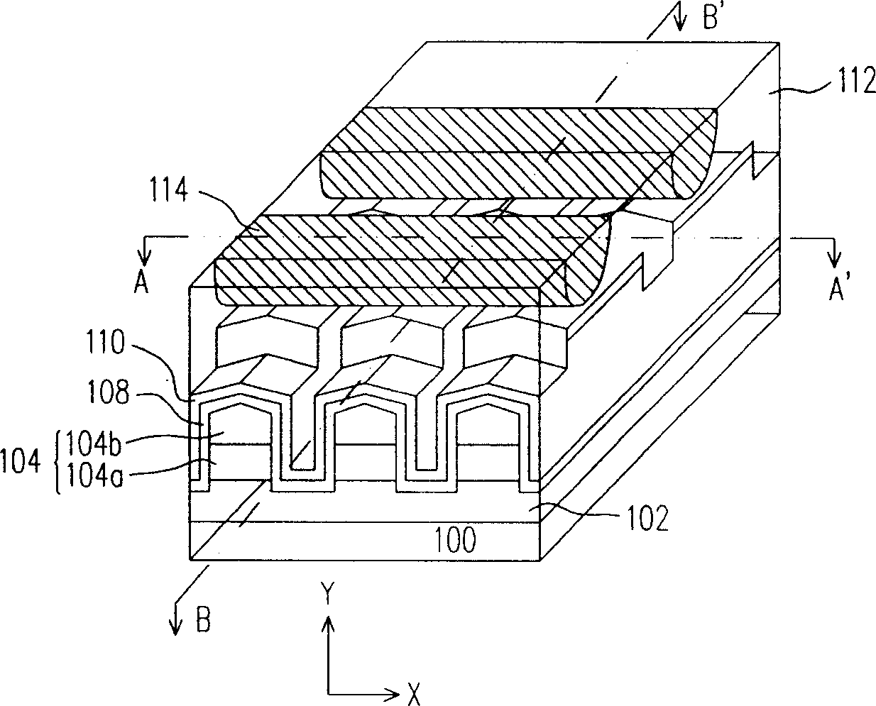
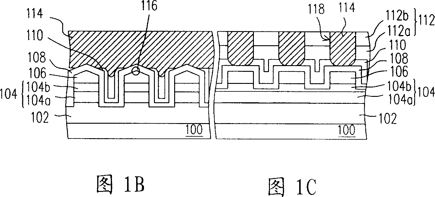
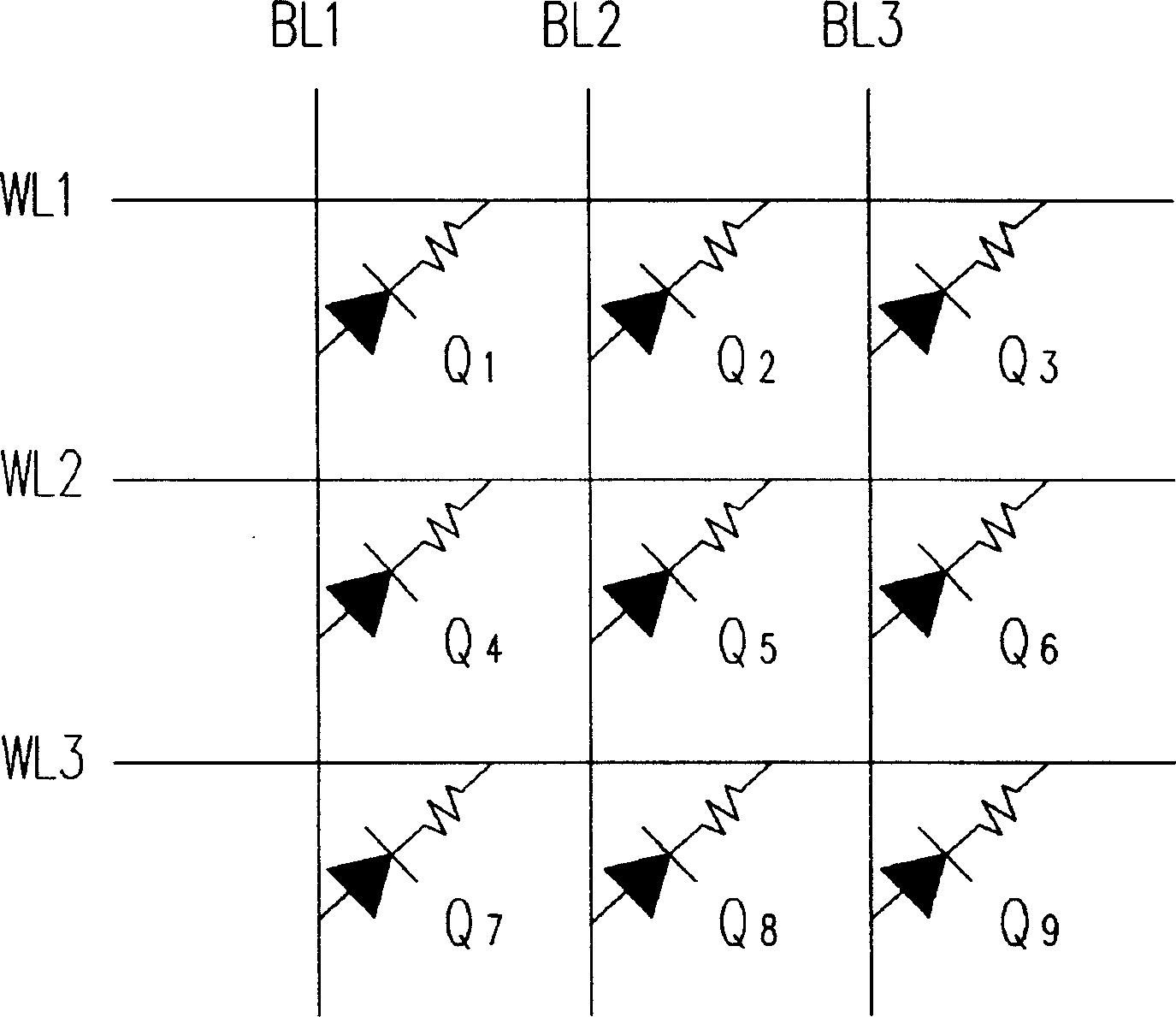
[0049] Figure 1A It is a three-dimensional structure diagram of the one-time programmable read-only memory in the first embodiment of the present invention. Figure 1B and Figure 1C are respectively Figure 1A The sectional view of the line A-A' and the sectional view of the line B-B'. Figure 1D It is a schematic diagram of an equivalent circuit of the one-time programmable read-only memory of the present invention.
[0050] see Figure 1A As shown in FIG. 1C, the one-time programmable read-only memory of the present invention is at least composed of a P-type semiconductor substrate 100, an N-type doped region 102, a P-type doped layer 104, an N-type doped layer 106, and an antifuse layer. 108 , an etching stop layer 110 , an interlayer insulating layer 112 , and a conductive layer 114 .
[0051] The N-type doped region 102 is disposed in the P-type semiconductor substrate 100 . The P-type doped layer 104 is disposed in the P-type semiconductor substrate 100 and located on ...
no. 2 example
[0085] Figure 10A It is a three-dimensional structure diagram of the one-time programmable read-only memory in the second embodiment of the present invention. Figure 10B and Figure 10C are respectively Figure 10A The sectional view of the line A-A' and the sectional view of the line B-B'. exist Figure 10A to Figure 10C, members with Figure 1A The same symbols as in FIG. 1C are given the same reference numerals, and description thereof will be omitted. Only the differences between this embodiment and the first embodiment are discussed here.
[0086] see Figure 10A Referring to FIG. 10C , in this embodiment, the antifuse layer 108 and the etch stop layer 110 are not directly sequentially disposed on the semiconductor substrate 100 (such as Figure 1A 1C ), but the interlayer insulating layer 112 is directly disposed on the semiconductor substrate 100 . The insulating layer 112 has a trench 118 directly exposing the N-type doped layer 106 . The antifuse layer 118 a is ...
no. 3 example
[0099] Figure 13A It is a three-dimensional structural schematic diagram of the one-time programmable read-only memory of the third embodiment of the present invention. Figure 13B and Figure 13C are respectively Figure 13A The sectional view of the line A-A' and the sectional view of the line B-B'. exist Figure 13A to Figure 13C, members with Figure 1A The same symbols as in FIG. 1C are given the same reference numerals, and description thereof will be omitted. Only the differences between this embodiment and the first embodiment and the second embodiment are discussed here.
[0100] see Figure 13A Referring to FIG. 13C , in this embodiment, the N-type doped layer 106a is not formed with sharp corners, but has a flat surface.
[0101] In the above-mentioned one-time programmable read-only memory, since the PN diode is formed in the semiconductor substrate 100, its material is a grown monocrystalline silicon semiconductor substrate, a crystalline silicon semiconductor...
PUM
 Abstract
Description
Claims
Application Information
 - R&D
- Intellectual Property
- Life Sciences
- Materials
- Tech Scout
- Unparalleled Data Quality
- Higher Quality Content
- 60% Fewer Hallucinations
Browse by: Latest US Patents, China's latest patents, Technical Efficacy Thesaurus, Application Domain, Technology Topic, Popular Technical Reports.
© 2025 PatSnap. All rights reserved.Legal|Privacy policy|Modern Slavery Act Transparency Statement|Sitemap|About US| Contact US: help@patsnap.com