Reaction chamber and semiconductor processing device

A reaction chamber and chamber wall technology, which is applied in semiconductor/solid-state device manufacturing, discharge tubes, electrical components, etc., can solve problems such as the size of the suspended support arm should not be too small, uneven air distribution, and asymmetric air flow path. To achieve the effect of flexible layout, simple structure and uniform air distribution

Active Publication Date: 2010-06-16
BEIJING NAURA MICROELECTRONICS EQUIP CO LTD
View PDF0 Cites 22 Cited by
  • Summary
  • Abstract
  • Description
  • Claims
  • Application Information

AI Technical Summary

Problems solved by technology

[0009] In prior art 1, since the air inlet is located on the side, it is arranged asymmetrically, resulting in uneven distribution of air flow on the surface of the substrate;
[0010] In the second prior art, in order to ensure sufficient strength and enough space for the installation of cooling devices, radio frequency devices and electrical circuits, etc., the size of the suspended support arm should not be too small, because the existence of the cantilever support causes the airflow path asymmetry, resulting in uneven air distribution

Method used


Image

  • Reaction chamber and semiconductor processing device
  • Reaction chamber and semiconductor processing device
  • Reaction chamber and semiconductor processing device

Examples


Embodiment Construction

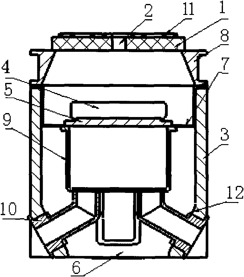
[0026] Reaction chamber of the present invention, its preferred embodiment one, as image 3 As shown, the chamber wall 3 is included, and the inner cavity of the reaction chamber is provided with a lower electrode box body 9, and the lower electrode box body 9 is supported on the chamber wall 3 through a plurality of channels 10, and the lower electrode box body 9 is supported on the chamber wall 3. The inner cavity communicates with the outside of the reaction chamber through a channel 10 ; the lower part of the chamber wall 3 is provided with a suction port 6 .

[0027] There can be 2 to 8 channels 10, such as 3 or 4 channels. A plurality of channels 10 may be evenly distributed circumferentially around the longitudinal axis of the reaction chamber to form a centrally symmetrical arrangement.

[0028] The specific structure can be that the reaction chamber is surrounded by the chamber wall 3, the dielectric window 1 and the dielectric window support 8, etc. to form a vacuum...


PUM


Abstract

The invention discloses a reaction chamber and a semiconductor processing device, in the reaction chamber, a lower electrode box body is supported on the chamber wall through a plurality of channels, and an inner cavity of the lower electrode box body is communicated with the outside of the reaction chamber through the plurality of channels; the plurality of channels are evenly distributed around the circumferential direction of the longitudinal axial line of the reaction chamber; and an air extraction port is formed at the lower part of the chamber wall. On the one hand, a centrally symmetric distribution structure is formed on an air extraction air passage, thereby forming even distribution of air flow; on the other hand, a variety of air pipelines, electrical lines, cooling pipelines, radio frequency lines and the like can be arranged through the plurality of channel, thereby realizing simple structure and flexible arrangement. The reaction chamber can be used for different types of semiconductor plasma processing, such as etching, deposition and the like.

Description

technical field [0001] The invention relates to semiconductor processing equipment, in particular to a reaction chamber for semiconductor processing. Background technique [0002] In the process of semiconductor processing, the reaction chamber provides a vacuum environment for the processing of semiconductor substrates. By supplying process gas to the reaction chamber and exciting the gas into a plasma state through a radio frequency power supply, the corresponding material corrosion or corrosion on the surface of the substrate is carried out. deposition and other processing techniques. [0003] For semiconductor substrate processing, the uniformity of the entire substrate surface treatment is an important indicator of the process. After the process gas enters the reaction chamber, a gas flow field is formed. The symmetry of the gas flow field relative to the center of the substrate is the key factor for the substrate surface treatment The key to the uniformity of the reac...

Claims


Application Information

Patent Timeline
Patent Type & Authority Applications(China)
IPC IPC(8): H01L21/00H01J37/32
Inventor 张风港
Owner BEIJING NAURA MICROELECTRONICS EQUIP CO LTD
Why Eureka
Try Eureka