Porous mask plate capable of being recognized by APS solar sensor
A solar sensor and mask technology, which is applied in the fields of instruments, optics, and photoengraving process of pattern surface, can solve the problems of unsuitable engineering application and complicated identification process, and achieves improvement of measurement accuracy, reduction of hardware resources, The effect of improving the data update rate
- Summary
- Abstract
- Description
- Claims
- Application Information
AI Technical Summary
Problems solved by technology
Method used
Image
Examples
Embodiment 1
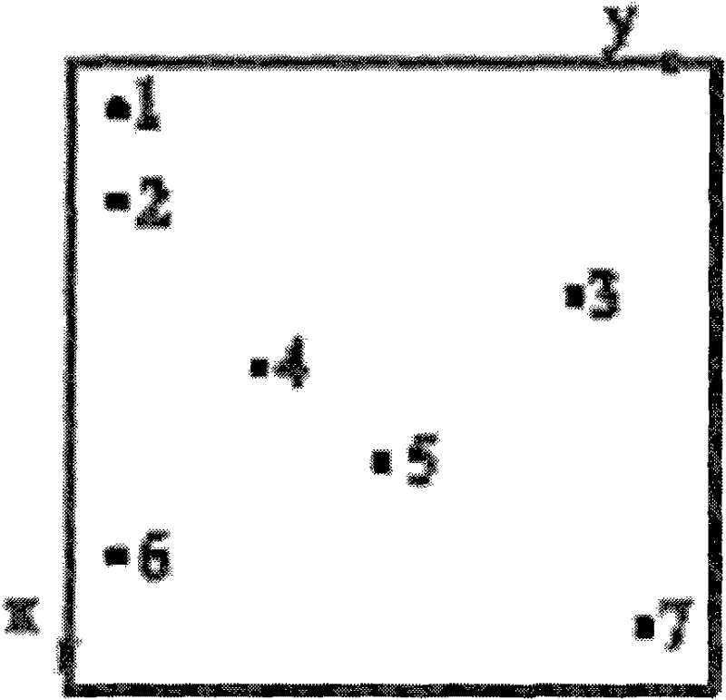
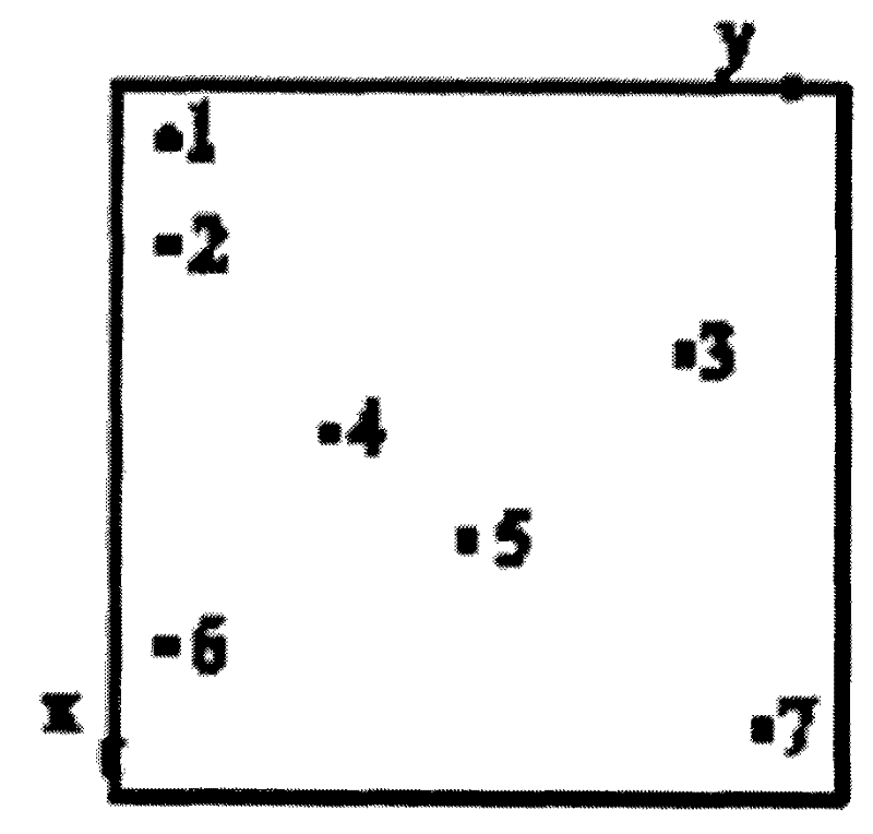
[0025] The invention solves the problem of identifying when the imaging holes in the imaging hole array of the porous mask plate are blocked by the APS imaging sun sensor due to the lunar dust environment during the landing and running stages of the lunar probe. In the moon dust environment, the sensor can be quickly and accurately identified when it is polluted by moon dust, and the polluted points can be eliminated through subsequent algorithms, so as to maintain high precision and high reliability when the sensor is polluted by moon dust.
[0026] Specifically divided into three aspects:
[0027] a. Determination of the imaging hole array scheme of the identifiable porous mask
[0028] b. Determination of the optimal pore size of the identifiable porous mask
[0029] c. Chromium coating with low reflectivity in laminated structure
[0030] The manufacturing process of the identifiable porous mask plate of the present invention will be described in detail below according t...
Embodiment 2
[0048] When the number of pinholes is 5, the distance between any two pinholes in the x direction and the distance in the y direction is 30 pixels, and the side length of the square area of the imaging pinhole is 4.05mm. The positional relationship between each small hole is shown in Table 2:
[0049] Table 2 Positional relationship between imaging pinholes
[0050] (x,y)
[0051] The plate-making process is the same as that in Example 1, and the mask plate is installed on the image sensor and assembled into a machine for testing. It is also measured that the measurement accuracy obtained by the APS sun sensor meets the requirements.
PUM
 Abstract
Description
Claims
Application Information
 - R&D
- Intellectual Property
- Life Sciences
- Materials
- Tech Scout
- Unparalleled Data Quality
- Higher Quality Content
- 60% Fewer Hallucinations
Browse by: Latest US Patents, China's latest patents, Technical Efficacy Thesaurus, Application Domain, Technology Topic, Popular Technical Reports.
© 2025 PatSnap. All rights reserved.Legal|Privacy policy|Modern Slavery Act Transparency Statement|Sitemap|About US| Contact US: help@patsnap.com


