Sigma-Delta analog-to-digital converter
An analog-to-digital converter and filter technology, applied in the field of integrated circuits, can solve the problems of large influence of process deviation, integrator operating frequency, settling time integration accuracy and power consumption deterioration, affecting the filtering accuracy of the analog-to-digital converter, etc. achieve the effect of avoiding adverse effects
- Summary
- Abstract
- Description
- Claims
- Application Information
AI Technical Summary
Problems solved by technology
Method used
Image

Examples
Embodiment 1
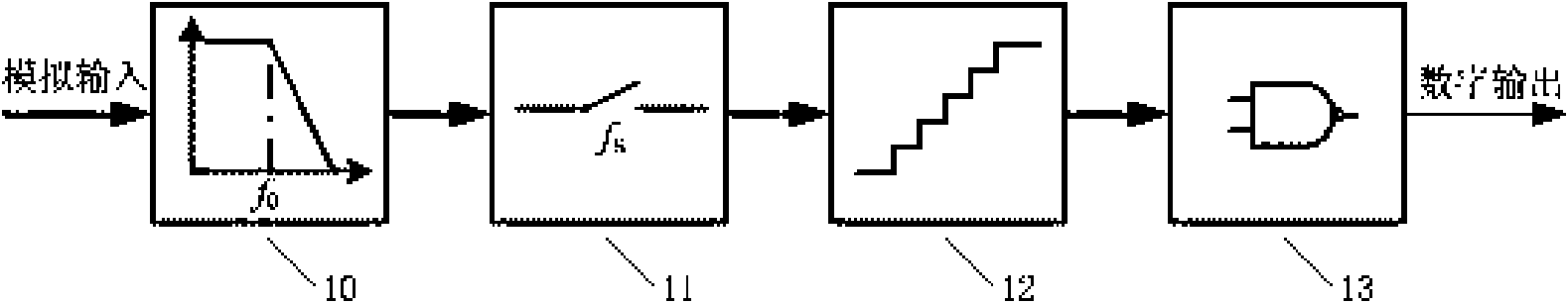
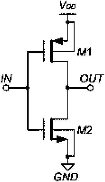
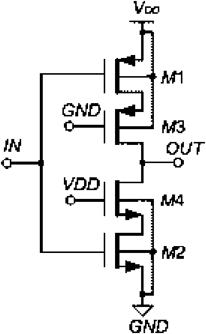
[0037] Embodiment one, the structural block diagram of the Sigma-Delta analog-to-digital converter of the present invention is as attached Figure 5 As shown, it includes a prior art anti-aliasing filter 50, a sample-and-hold 51, a digital decimation filter 53 and an innovative analog modulator 52 of the present invention. The sample-and-hold 51 is used for over-sampling of the analog input signal to reduce quantization noise within the signal bandwidth, and the analog modulator 52 is used for noise shaping during the analog-to-digital conversion process. Oversampling and noise shaping are two key technologies of Sigma-Delta ADC. The analog modulator 52 adopts a new class C inverter (hereinafter the same) with the application number of 2009103013271 (patent name: class C inverter using a body potential modulator) to replace the traditional operational amplifier or the class C inverter of the prior art. Inverter, the new class C inverter is based on the class C inverter 40 of ...
Embodiment 2
[0051] Embodiment 2. The third-order single-ring structure Sigma-Delta analog-to-digital converter proposed by the present invention is characterized in that the analog modulator is a third-order single-ring structure. attached Figure 7 It is a structural block diagram of a third-order single-loop analog modulator, which includes three pseudo-differential structure switched capacitor integrators 70, 71 and 72, and two adders 54, 73 and a coarse quantizer 56 of the prior art. Wherein three integrators 70, 71 and 72 are sequentially connected in series on a single loop to form a loop filter 55, and the coarse quantizer 56 includes a feed-forward ADC 56a and a feedback DAC 56b, which can be used in combination with the loop filter 55 to realize a third-order noise shaping and precise analog-to-digital conversion. c1, c2 and c3 are scaling factors of the modulator, which are used to scale the signal so that within the input range of the modulator, the output swing of the integra...
PUM
 Abstract
Description
Claims
Application Information
 - R&D
- Intellectual Property
- Life Sciences
- Materials
- Tech Scout
- Unparalleled Data Quality
- Higher Quality Content
- 60% Fewer Hallucinations
Browse by: Latest US Patents, China's latest patents, Technical Efficacy Thesaurus, Application Domain, Technology Topic, Popular Technical Reports.
© 2025 PatSnap. All rights reserved.Legal|Privacy policy|Modern Slavery Act Transparency Statement|Sitemap|About US| Contact US: help@patsnap.com