Eureka AIR delivers breakthrough ideas for toughest innovation challenges, trusted by R&D personnel around the world.

Semiconductor single crystal production apparatus

Inactive Publication Date: 2010-08-26
SUMCO TECHXIV
View PDF5 Cites 11 Cited by
  • Summary
  • Abstract
  • Description
  • Claims
  • Application Information

AI Technical Summary

Benefits of technology

[0022]The present invention is created with the foregoing in view, and a first problem to be resolved by the present invention is to increase the quality of a low-resistance semiconductor single crystal doped to a high concentration with an N-type volatile dopant and increase the production yield of the single crystal by controlling the pressure inside the furnace with good controllability.

Problems solved by technology

Thus, because the pressure in the sub-vacuum region is from the beginning higher than that in the normal furnace pressure region, the pressure inside the furnace rapidly rises to an abnormal pressure.

Method used


Image

  • Semiconductor single crystal production apparatus
  • Semiconductor single crystal production apparatus
  • Semiconductor single crystal production apparatus

Examples


first embodiment

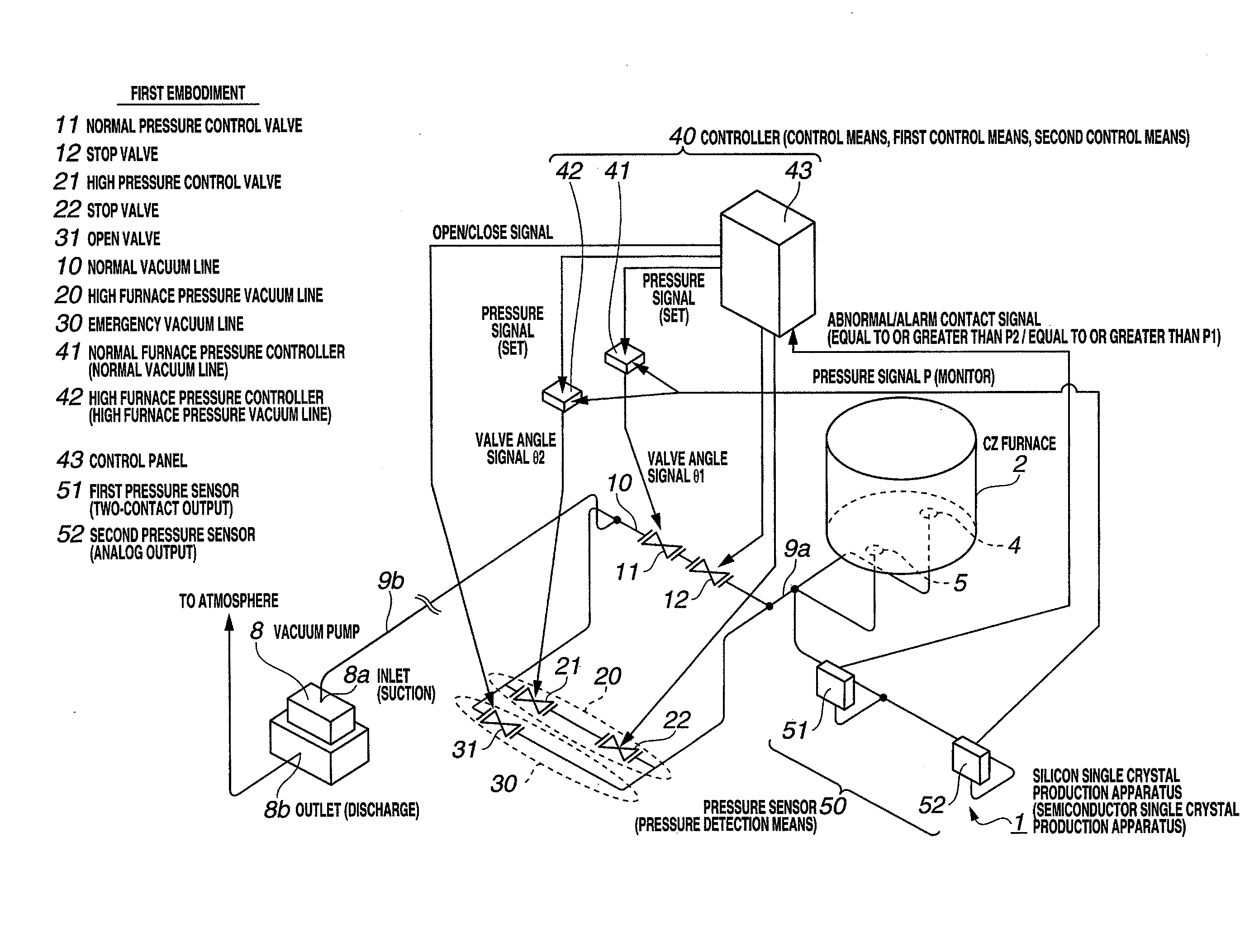
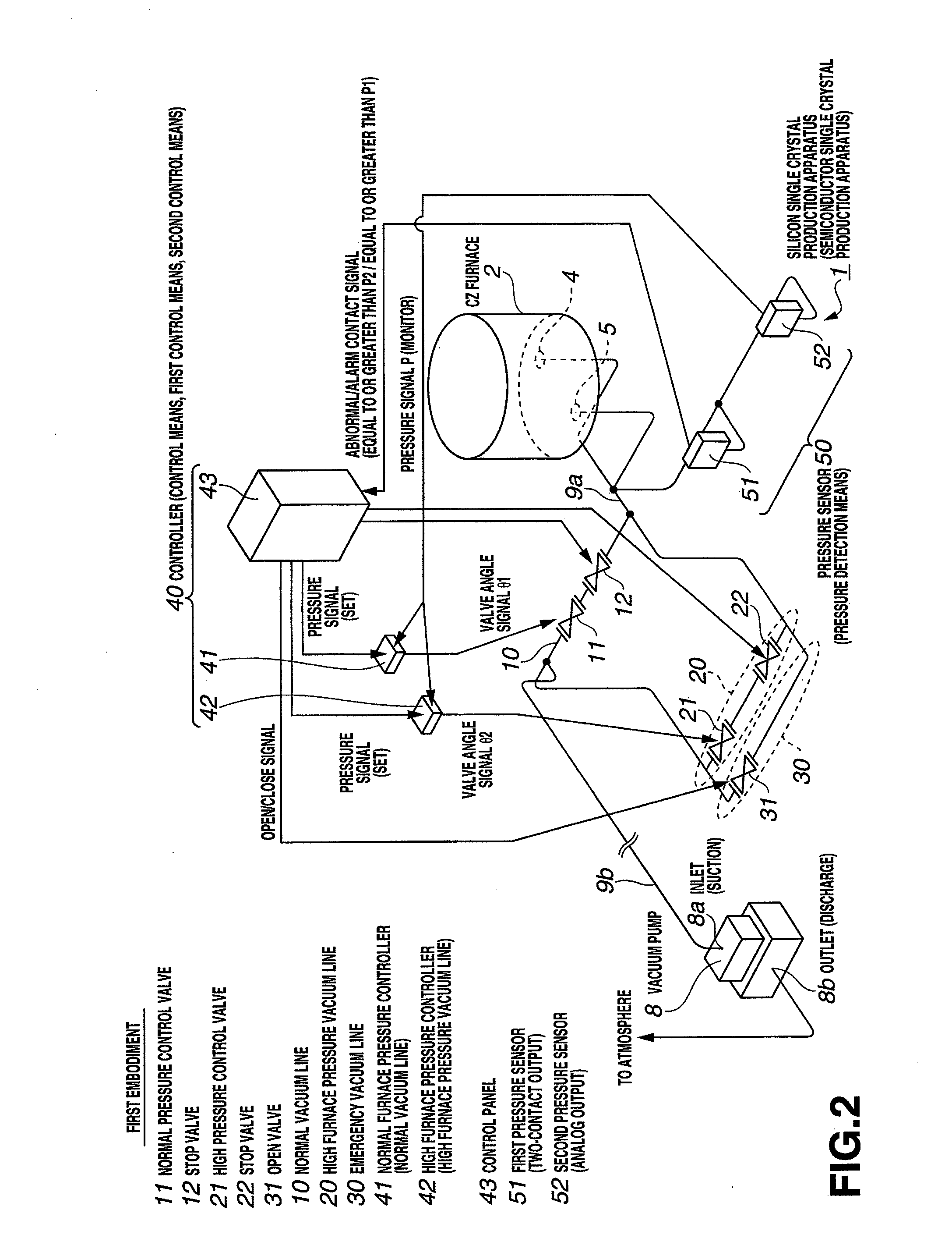
[0090]FIG. 2 shows the configuration of a silicon single crystal production apparatus 1 of the embodiment. The apparatus 1 of this embodiment serves to produce a volatile N-type high-concentration and low-resistance silicon wafer (high furnace pressure product) and a silicon wafer (normal furnace pressure product) with a concentration lower and a resistance higher than those of the high furnace pressure product. The silicon single crystal production apparatus 1 is installed in a clean room.

[0091]The “N-type volatile dopant” as referred to herein is antimony Sb, red phosphorus P, and arsenic As, etc. The “low resistance” is taken as a resistance value that is equal to or lower than 20 / 1000 Ωcm.

[0092]Outlets (discharge) 4, 5 of a CZ furnace 2 are provided on the lower side of the CZ furnace 2. In the present embodiment, a structure is assumed in which gas is discharged from the lower side of the CZ furnace 2, but gas outlets (discharge) may be provided in any location of the CZ furnac...

second embodiment

[0168]FIG. 5 shows a configuration in which, compared with FIG. 2, normal vacuum line 10 and emergency vacuum line 30 except for the high furnace pressure vacuum line 20 are omitted and only the high furnace pressure vacuum line 20 is provided as a vacuum line linking the CZ furnace 2 to the vacuum pump 8.

[0169]With the second embodiment, the above-described effect A can be obtained.

third embodiment

[0170]FIG. 6 shows a configuration in which, compared with FIG. 2, normal vacuum line 10 except for the high furnace pressure vacuum line 20 and emergency vacuum line 30 is omitted and only the high furnace pressure vacuum line 20 and emergency vacuum line 30 are provided as vacuum lines linking the CZ furnace 2 to the vacuum pump 8.

[0171]With the third embodiment, the above-described effects A and B can be obtained.


PUM


Abstract

An apparatus designed to increase the quality of a low-resistance semiconductor single crystal doped with an N-type volatile dopant to a high concentration and increase the production yield by controlling the pressure inside the furnace with good controllability. A vacuum line, a pressure control valve, and an open valve are newly added to the conventional semiconductor single crystal production apparatus. A controller controls the pressure control valve on the basis of a detection value of pressure detection means so as to obtain the desired low resistance value of the semiconductor single crystal. The open valve is controlled so that the open valve is opened in a case where the pressure inside the furnace detected by the pressure detection means reaches an abnormal value.

Description

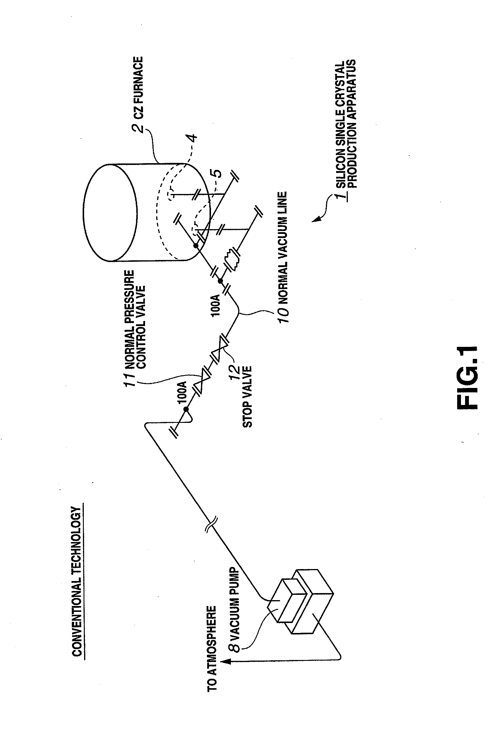
TECHNICAL FIELD[0001]The present invention relates to a semiconductor single crystal production apparatus, and more particularly to an apparatus in which an inert gas is supplied in a furnace and a semiconductor single crystal doped with a dopant is produced inside the furnace, while discharging the gas in the furnace from an outlet (discharge) via a vacuum line.BACKGROUND ARTConventional Technology[0002]A demand was created in recent years for high-yield production of silicon wafers for use in discrete semiconductor devices and the like, namely, low-resistance silicon wafers that have N-type electric characteristics and are doped to a high concentration with a volatile dopant.[0003]Examples of N-type volatile dopants referred to herein include antimony Sb, red phosphorus P, and arsenic As. The low resistance is a resistance value equal to or lower than 20 / 1000 Ωcm.[0004]FIG. 1 shows a configuration of a conventional silicon single crystal production apparatus 1. This conventional a...

Claims


Application Information

Patent Timeline
IPC IPC(8): H01L21/365
CPCC30B29/06C30B15/20
Inventor SUDA, AYUMIMITANI, NAOJI
Owner SUMCO TECHXIV
Why Eureka
Eureka Blog
Learn More