
Method for processing multilayer flexible circuit board

A technology of flexible circuit boards and processing methods, which is applied in multilayer circuit manufacturing, printed circuit, printed circuit manufacturing, etc., can solve problems affecting processing quality, expansion and contraction of inner layer circuit board copper foil, cover film bubbles, etc., to reduce The effect of drilling position deviation probability, improving single product yield, and reducing the probability of short circuit

Inactive Publication Date: 2011-07-13
靖江亚星进出口有限公司
View PDF0 Cites 0 Cited by
  • Summary
  • Abstract
  • Description
  • Claims
  • Application Information

AI Technical Summary

Problems solved by technology

[0036] 1. Since all the bending areas of the inner circuit board are punched off in step 203, the hollowed-out area of ​​the inner circuit board copper foil is relatively large, so that the inner circuit board copper foil has more serious defects in the subsequent process. expansion and contraction phenomenon;
[0037] 2. Due to the relatively serious expansion and contraction phenomenon of the copper foil of the inner layer circuit board, the position of each outer layer circuit on the copper foil of the outer layer circuit board will deviate from the corresponding drilling position of the inner layer circuit, thereby affecting the drilling in step 206. The processing quality of the hole process;
[0038] 3. Due to the large hollow area of ​​the inner circuit board copper foil, the bending area of ​​the outer circuit board copper foil that is composited with the inner circuit board copper foil corresponding to the hollow will be depressed, so that the outer circuit board copper foil is in the corresponding There are steps at the edge of the bending area at the hollowed out part, so that the phenomenon of poor exposure will occur in step 207, and bubbles will appear in the cover film when the outer cover film is hot-pressed in step 208
[0039] All of the above problems may lead to short circuit, which seriously reduces the single-product yield of multilayer flexible circuit boards

Method used


Image

  • Method for processing multilayer flexible circuit board
  • Method for processing multilayer flexible circuit board
  • Method for processing multilayer flexible circuit board

Examples


Embodiment Construction

[0068] In order to make the objectives, technical solutions, and advantages of the present invention clearer, the following further describes the present invention in detail with reference to the accompanying drawings and embodiments.

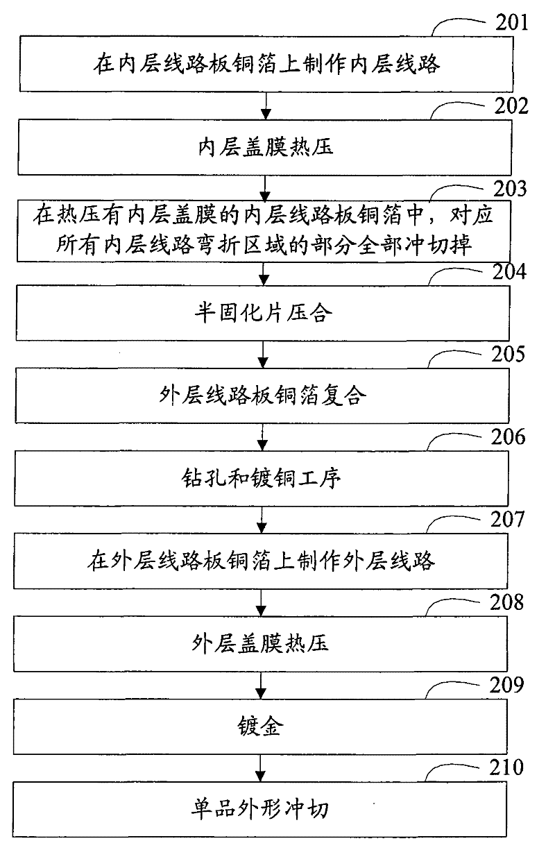
[0069] Figure 5 It is a schematic flow diagram of the method for processing a multilayer flexible circuit board in the present invention. Such as Figure 5 As shown, the processing method of the multilayer flexible circuit board in the present invention includes the following steps:

[0070] In step 501, multiple single-product inner-layer circuits are made on the copper foil of the inner-layer circuit board.

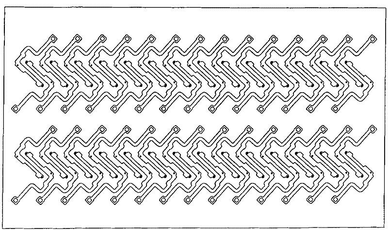
[0071] This step can specifically include dry film lamination, exposure, development, and etching. The inner circuit board copper foil processed by this step contains multiple single-product inner circuit and inner circuit board copper foil. Please refer to the layout styles of multiple inner lines on the image 3 .

[0072] In practical appli...


PUM


Abstract

The invention discloses a method for processing a multilayer flexible circuit board, which comprises the following steps: punching a notch at two ends of a bended area of an inner layer circuit copper foil hot-pressed with an inner layer covering film respectively; reserving most of the bended area of an inner layer circuit in the subsequent process steps; and taking out reserved most of the bended area of the inner layer circuit until the last process step so that the hollow cut area of the inner layer circuit board copper foil in the subsequent process steps is reduced, the swelling and shrinking ratio of the inner layer circuit board copper foil in the subsequent process steps is reduced, and furthermore, the probability for each outer layer circuit on an outer layer circuit board copper foil to deviate from a corresponding drilling position of the inner layer circuit is reduced. Besides, in the subsequent process steps, the bended area of the outer layer circuit board copper foil compounded to the inner layer circuit board copper foil is not sunken to avoid steps appearing at the edge of the bended area of the outer layer circuit board copper foil so as to avoid the phenomenonof bad exposure and bubbles appearing in the covering film when the covering film is in hot pressing.

Description

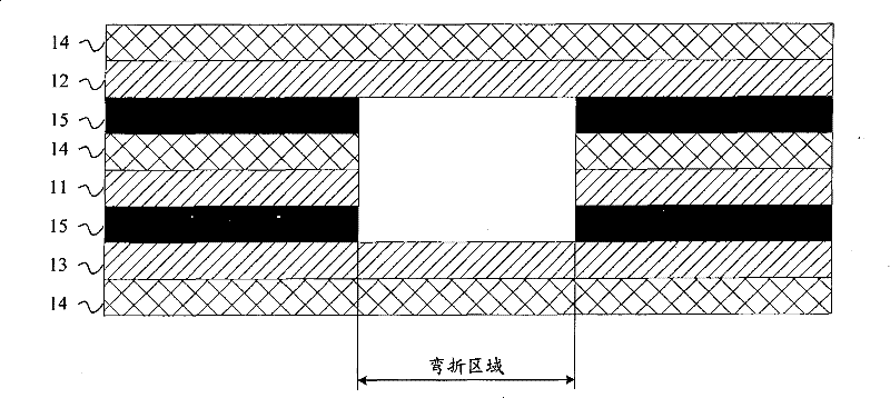
Technical field [0001] The invention relates to a flexible circuit board processing technology, in particular to a processing method of a multilayer flexible circuit board. Background technique [0002] The multi-layer flexible circuit board is formed by superimposing a plurality of single-layer flexible circuit boards. The single-layer flexible circuit board described here may be a single-sided single-layer flexible circuit board or a multi-sided single-layer flexible circuit board. [0003] figure 1 It is a side sectional view of an existing three-layer flexible circuit board. Such as figure 1 As shown, the three-layer flexible circuit board includes from top to bottom: cover film 14, first outer layer copper foil 12, prepreg 15, cover film 14, inner layer copper foil 11, prepreg 15, and second outer layer copper foil 13. Cover film 14. [0004] Among them, the inner layer of copper foil 11 is processed by exposure, development, etching, etc., as the inner layer circuit board of ...

Claims


Application Information

Patent Timeline
Patent Type & Authority Patents(China)
IPC IPC(8): H05K3/46H05K3/00
Inventor 顾志明韩垂华
Owner 靖江亚星进出口有限公司
Learn More