High anti-static Schottky diode
A Schottky diode, electrostatic technology, applied in circuits, electrical components, electrical solid devices, etc., can solve the problems of weak metal barrier withstand surge, Schottky diode failure, and metal barrier electrostatic damage.
- Summary
- Abstract
- Description
- Claims
- Application Information
AI Technical Summary
Problems solved by technology
Method used
Image
Examples
Embodiment
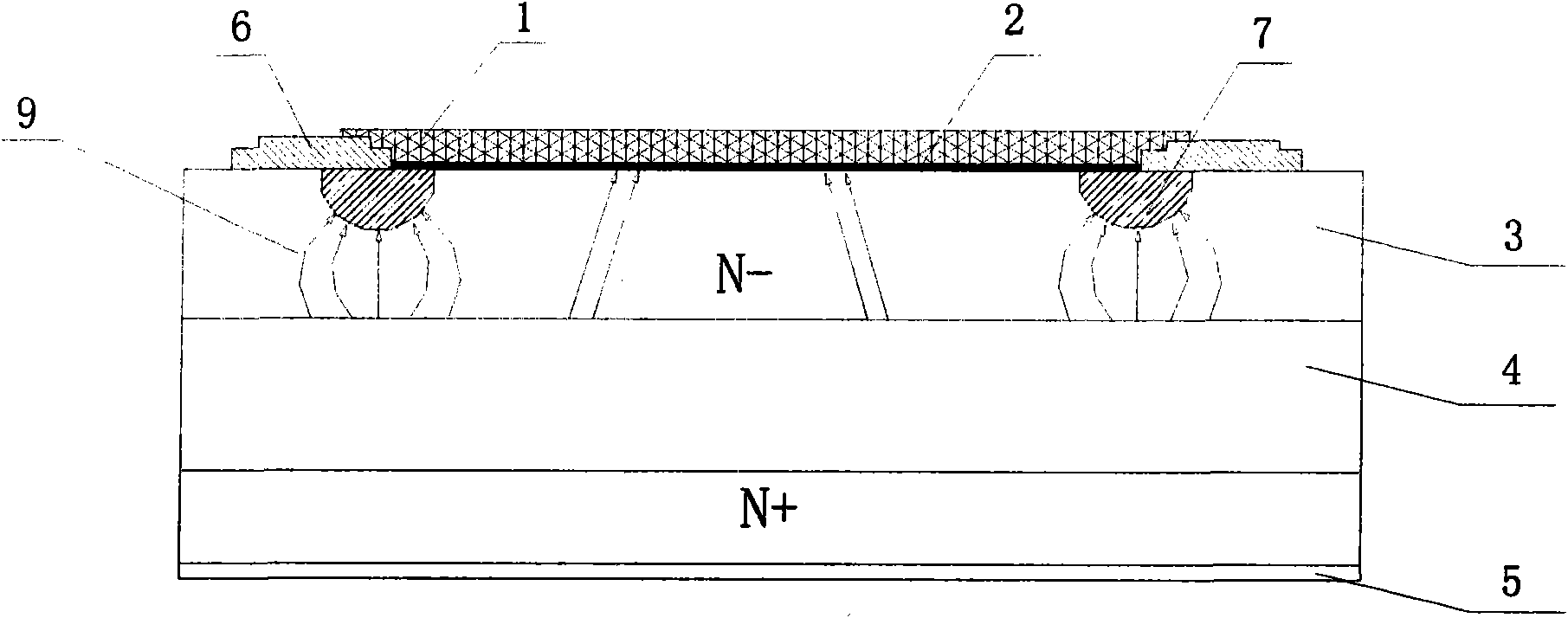
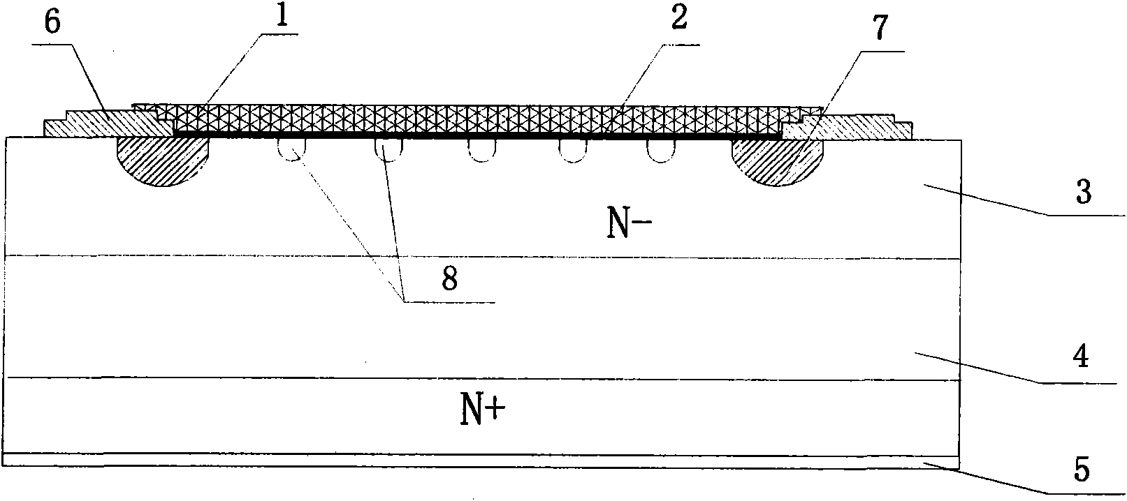
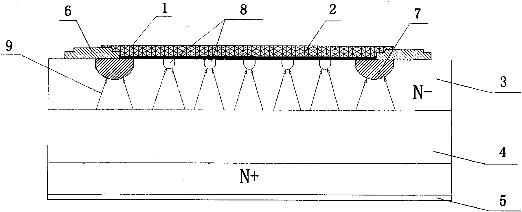
[0014] Example: such as figure 2 As shown, the high antistatic Schottky diode of the present invention is based on an N-type semiconductor as a substrate 4; an N-epitaxial layer 3, a metal barrier layer 2 and an anode metal layer 1 are formed using phosphorus as a dopant; Silicon dioxide (SiO 2 ) 6 is used to eliminate the electric field in the edge region and improve the withstand voltage of the tube; an N+ cathode layer and a cathode metal layer 5 for reducing the contact resistance of the cathode are formed under the substrate 4 . Among them, the anode metal layer 1 is a barrier layer made of materials such as molybdenum or aluminum; a P-type protective ring 7 is also provided on the N-epitaxial layer 3 to form a protective diode; The boron atoms are diffused in one direction to form a P-type boron diffusion region 8, and form six evenly distributed P-type lattice diodes with the N-epitaxial layer 3, which are connected in parallel with the protection diodes formed by the ...
PUM
 Abstract
Description
Claims
Application Information
 - R&D Engineer
- R&D Manager
- IP Professional
- Industry Leading Data Capabilities
- Powerful AI technology
- Patent DNA Extraction
Browse by: Latest US Patents, China's latest patents, Technical Efficacy Thesaurus, Application Domain, Technology Topic, Popular Technical Reports.
© 2024 PatSnap. All rights reserved.Legal|Privacy policy|Modern Slavery Act Transparency Statement|Sitemap|About US| Contact US: help@patsnap.com


