Recognition mark, and circuit substrate manufacturing method

A technology of identification marks and manufacturing methods, applied in the field of identification marks

Inactive Publication Date: 2012-12-05
PANASONIC CORP
View PDF4 Cites 0 Cited by
  • Summary
  • Abstract
  • Description
  • Claims
  • Application Information

AI Technical Summary

Problems solved by technology

However, when the identification mark 27 is processed on the above-mentioned prepreg 21, if the laser beam is deflected, the hole diameters of the conductive paste 24 on the incident side and the outgoing side in the same direction will be different, and it will be the same as the case of forming a single through hole. center of gravity shift

Method used


Image

  • Recognition mark, and circuit substrate manufacturing method
  • Recognition mark, and circuit substrate manufacturing method
  • Recognition mark, and circuit substrate manufacturing method

Examples


Embodiment approach

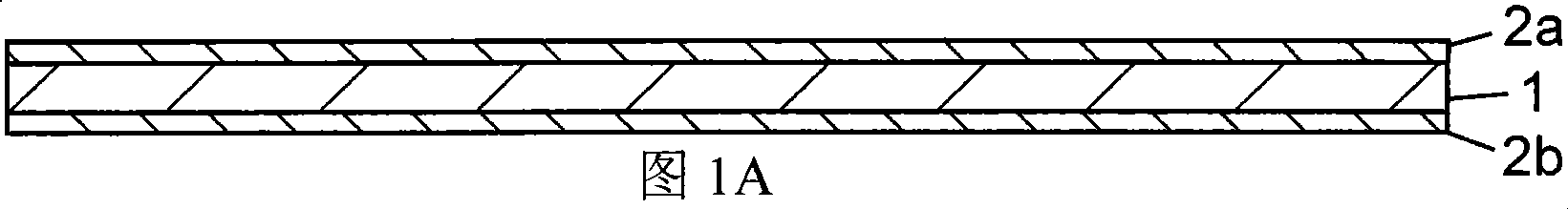
[0122] first as Figure 1A As shown, the release films 2a, 2b are attached to the front and back surfaces of the prepreg 1 using a laminating device.

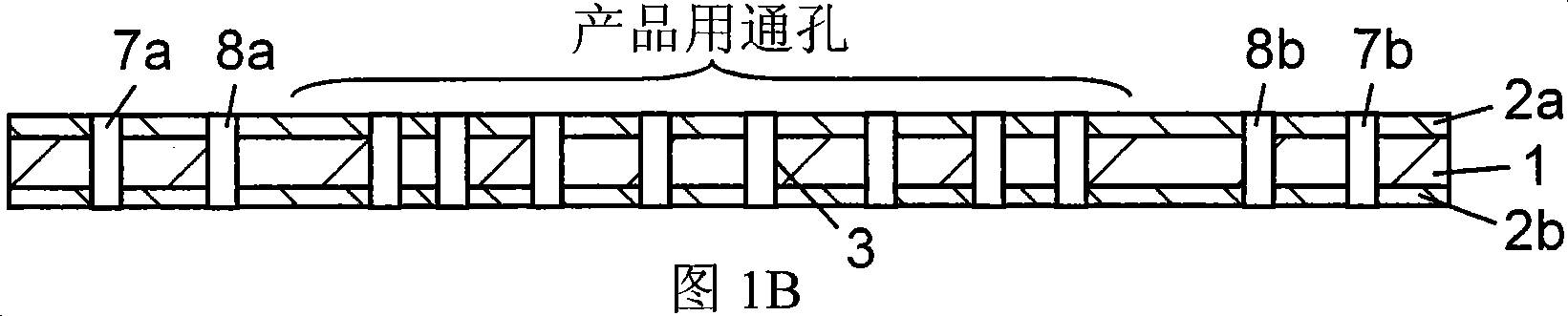
[0123] The prepreg 1 uses a base material formed of a composite material such as wholly aromatic polyamide fiber or glass fiber cloth of a nonwoven fabric impregnated with a thermosetting epoxy resin. A laminating device is used to bond a plastic film having a release layer portion formed on the front and back surfaces of the prepreg 1 , for example, release films 2 a , 2 b made of polyethylene terephthalate or the like.

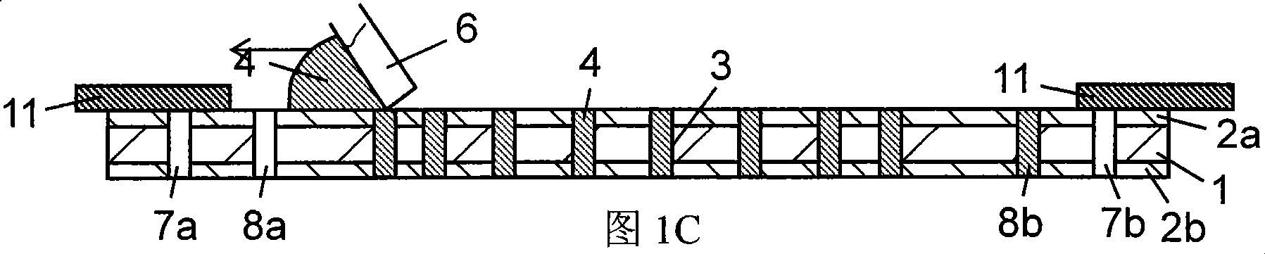
[0124] Secondly, if Figure 1B As shown, via holes 3 serving as internal via holes are formed by laser processing or the like. At this time, while forming the via hole 3 for the product (that is, for interlayer connection), the via hole 7a, 7b for the lamination identification mark not filled with the conductive paste 4 described below is formed by laser processing, and the via hole 7b for the thermal press...


PUM

PropertyMeasurementUnit
aperture sizeaaaaaaaaaa

Abstract

Through hole (3) for product, through holes (7a, 7b) for laminate recognition marks, through holes (8a, 8b) for an X-ray recognition marks are formed on prepreg sheet (1) having mold release films (2a, 2b) attached to the front and back surfaces thereof. By masking through holes (7a, 7b) for laminate recognition mark, conductive paste (4) is filled in through hole (3) for product and through holes (8a, 8b) for X-ray recognition marks. Thereafter, mold release films (2a, 2b) are removed so as to manufacture a circuit board. Since conductive paste (4) is not filled in through holes (7a, 7b) for laminate recognition marks, a recognition mark with high laminating accuracy can be easily obtained, and a high density and high quality circuit formation substrate having improved laminating accuracy can be obtained.

Description

technical field [0001] The present invention relates to identification marks used when manufacturing circuit boards used in various electronic devices, and the present invention relates to a method of manufacturing circuit boards using the identification marks. Background technique [0002] In recent years, as electronic equipment tends to be miniaturized and denser, circuit substrates carrying electronic components have also developed from existing single-sided substrates to double-sided and multi-layer substrates, and have developed a new technology that can integrate more High-density substrates with many circuits and parts. [0003] In particular, as the density of multilayer substrates increases, circuit patterns become finer, and circuit patterns of more layers and thinner substrates are required. [0004] In such a circuit board, it is necessary to newly develop a connection method for connecting circuit patterns of multiple layers through internal via holes using a ...

Claims


Application Information

Patent Timeline
Patent Type & Authority Patents(China)
IPC IPC(8): H05K1/02H05K1/11H05K3/00H05K3/40H05K3/46
CPCH05K3/4652H05K3/4638H05K2201/10378H05K2203/0242H05K3/4069H05K3/0047H05K2201/09781H05K2203/1136H05K2201/0355H05K2201/0323H05K1/0269H05K2201/09981H05K2203/1461H05K3/0032H05K3/4679H05K2201/09063H05K2201/09918H05K3/4614H05K2203/0191
Inventor 竹中敏昭平石幸弘冈本孝雄马田督也
Owner PANASONIC CORP
Why Eureka
Try Eureka