Method and device for manufacturing optical display device

a technology of optical display and manufacturing method, which is applied in the direction of lamination ancillary operations, instruments, chemistry apparatus and processes, etc., can solve the problems of high laminating accuracy, cycle time, and high manufacturing speed of optical film sheets, and achieve high laminating accuracy

Inactive Publication Date: 2019-02-05
NITTO DENKO CORP
View PDF8 Cites 0 Cited by
  • Summary
  • Abstract
  • Description
  • Claims
  • Application Information

AI Technical Summary

Benefits of technology

[0014]An aim of the present invention is to provide a method and an apparatus for manufacturing an optical display device with high laminating accuracy, as mentioned above.
[0021]The above-mentioned technical problem may be solved by, after completing lamination of an optical film sheet and a panel component, reading a rear end of a next optical film sheet supported on a carrier film in a state where one of opposite surfaces thereof is folded to inside at a tip-end of a peeling member and passed around the peeling member as positional information at a predetermined detecting position, and while peeling an optical film sheet from a carrier film, based on the positional information, determining winding length of the carrier film such that the rear end of the optical film sheet is positioned to a predetermined laminating position. By this, lamination error may be minimized without sacrificing cycle time per a panel component by leveling lamination error due to curl or droop generated at a leading end of an optical film sheet in a head-out state.

Problems solved by technology

Roll length of such an optical film laminate is about 900 m. However, manufacturing speed i.e., cycle time for such middle- or small-sized liquid-crystal display device is required to be two times higher than that for a large liquid-crystal display device, and laminating accuracy for an optical film sheet, such as a polarizing film supported on a carrier film, to be laminated to a liquid-crystal panel LC is also very severe.

Method used


Image

  • Method and device for manufacturing optical display device
  • Method and device for manufacturing optical display device
  • Method and device for manufacturing optical display device

Examples


Embodiment Construction

(Outline of a Method for Manufacturing an Optical Display Device and an Apparatus Therefor)

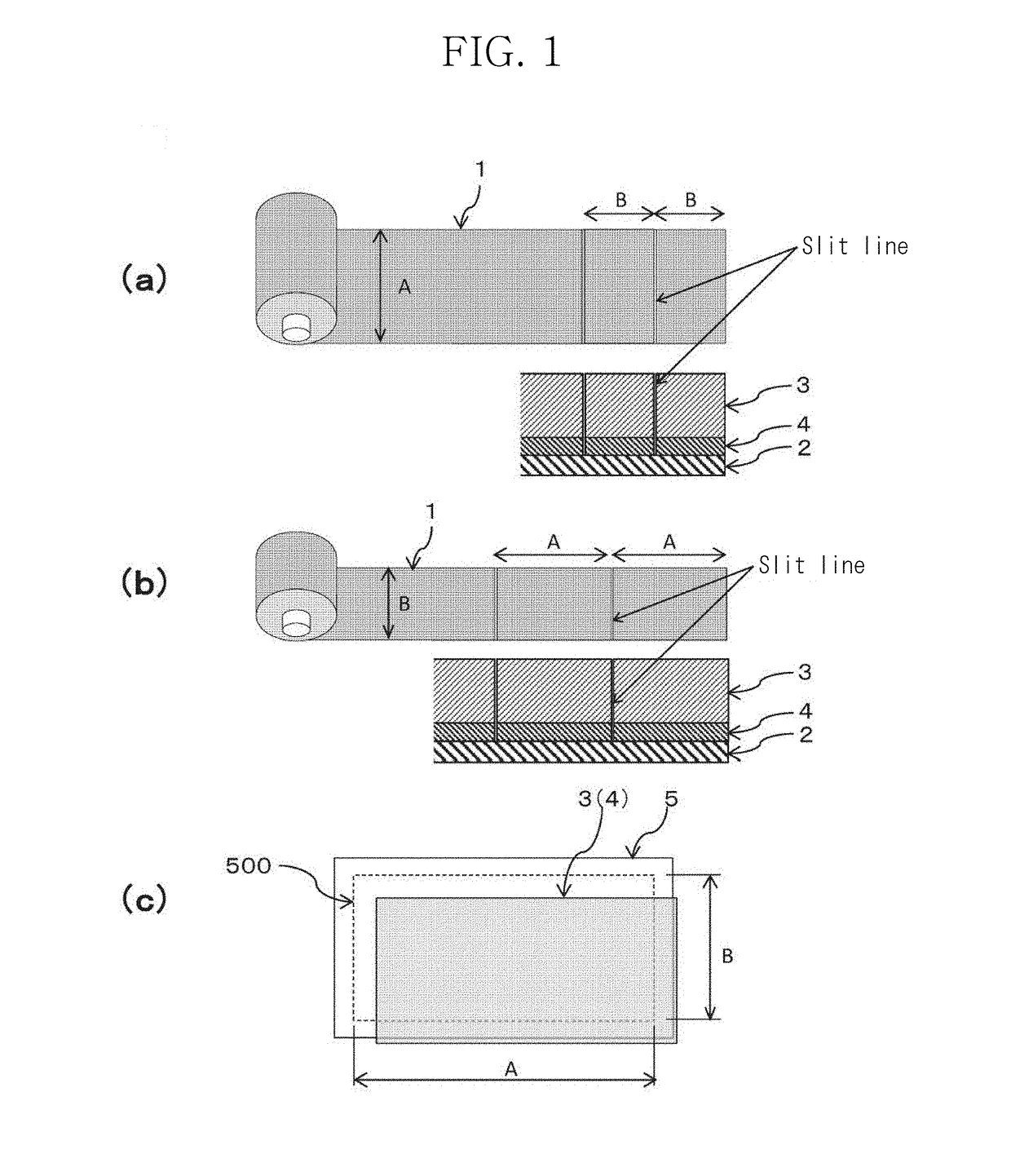
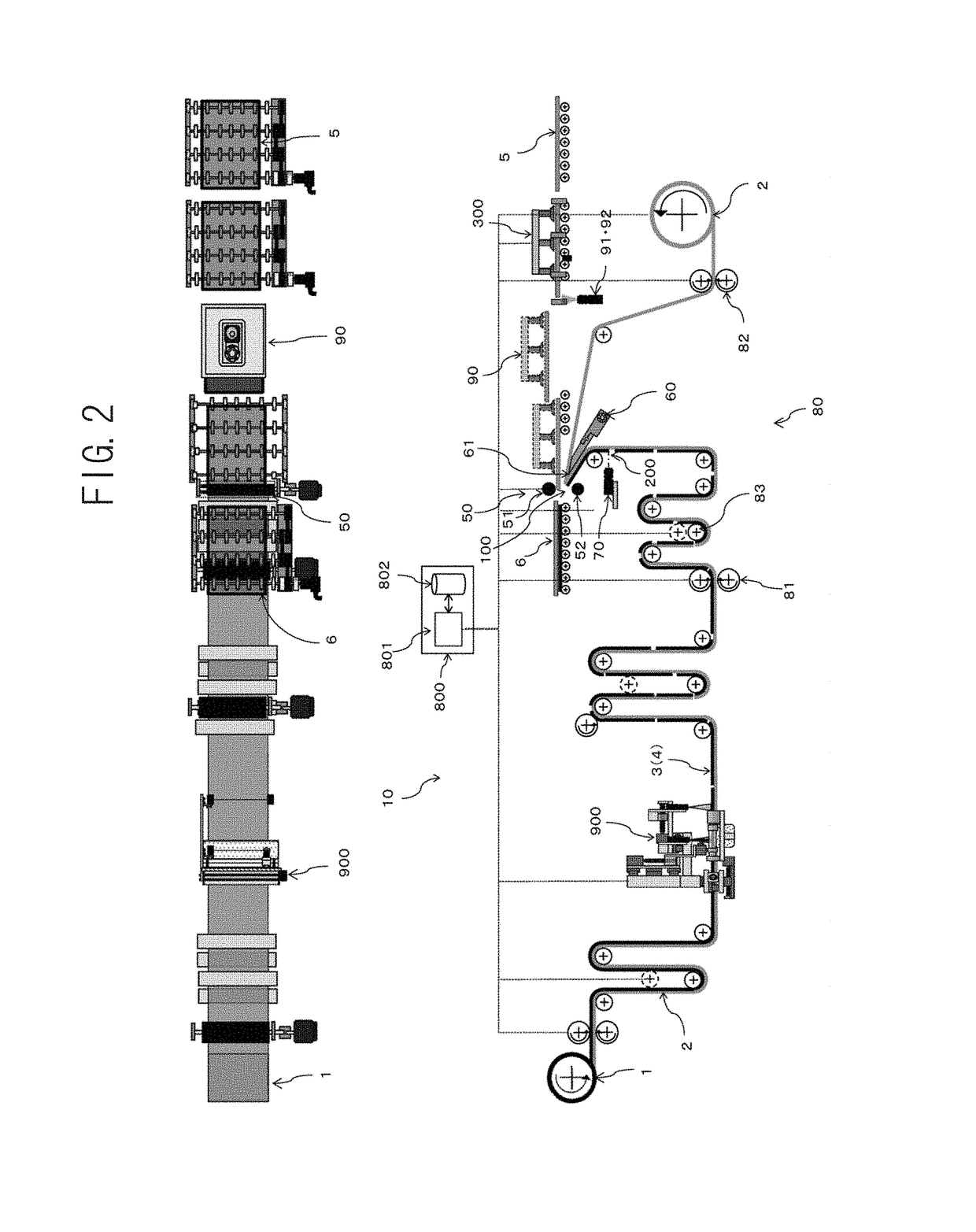
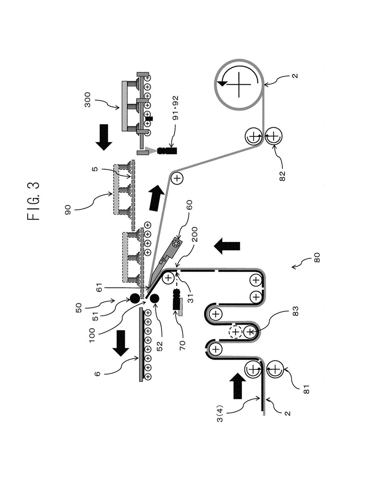
[0061]FIG. 2 illustrates a top view and a side view showing an entire apparatus 10 for manufacturing an optical display device 6 by laminating an optical film sheet 3 and a panel component 5 at a predetermined laminating position 100. As shown in FIG. 1, the optical film sheet 3 including an adhesive layer 4 is formed by forming a plurality of slit lines by a slitting unit 900 shown in FIG. 2 on an optical film laminated together with an adhesive layer 4 on one of opposite surfaces of a long web of a carrier film 2 which configures an optical film laminate 1 with a width corresponding to a long side A or a short side B of a laminating surface 500 formed by leaving edges at a long side a and a short side b of the panel component 5 having rectangular shape.

[0062]The apparatus 10 used in an embodiment of the present invention may be, for example but not limited to, an apparatus configuring a part...


PUM

PropertyMeasurementUnit
sizeaaaaaaaaaa
sizeaaaaaaaaaa
weightaaaaaaaaaa

Abstract

A method and an apparatus for manufacturing an optical display device by sequentially peeling a plurality of optical film sheets continuously supported on a long web of a carrier film and laminating the plurality of optical film sheets to a plurality of panel components are provided. After completing laminating operation of a preceding optical film sheet to a preceding panel component, a rear end of next optical film sheet, supported on a carrier film which in a state where one of opposite surfaces thereof is folded to inside at a tip-end of a peeling member, is read at a predetermined detecting position as positional information, then a leading end of an optical film sheet is positioned at a predetermined laminating position based on the positional information while peeling the optical film sheet from the carrier film.

Description

CROSS REFERENCE TO RELATED APPLICATION[0001]This application claims the priority of Japanese Patent Application No. 2013-197999, filed on Sep. 25, 2013 in the JPO (Japanese Patent Office). Further, this application is the National Phase application of International Application No. PCT / JP2013 / 076468 filed Sep. 30, 2013, which designates the United States and was published in Japanese.TECHNICAL FIELD[0002]The present invention relates to a method and an apparatus for manufacturing an optical display device. In particular, the present invention relates to a method and an apparatus, which use a peeling member having a tip-end, for manufacturing an optical display device for sequentially peeling a plurality of optical film sheets continuously supported via an adhesive layer on one of opposite surfaces of a carrier film together with the adhesive layer from the carrier film under peeling action of a peeling member and winding operation of a long web of a carrier film in a state where the ...

Claims


Application Information

Patent Timeline
Patent Type & Authority Patents(United States)
IPC IPC(8): B32B37/12G02F1/13B32B38/10G02F1/1335B32B38/00G02F1/1333
CPCG02F1/1303B32B37/12B32B38/0004B32B38/10G02F1/1335G02F2202/28B32B2457/202B32B2551/00G02F2001/133354G02F1/133354
Inventor YURA, TOMOKAZUKOSHIO, SATORUTSUTSUMI, KIYOTAKA
Owner NITTO DENKO CORP
Why Eureka
Try Eureka