
Manufacturing method of wide-spectrum high-power semiconductor superradiance LED

A superluminescence, high-power technology, applied in semiconductor devices, electrical components, circuits, etc., can solve the problems that superluminescence diodes cannot meet the requirements of high power and wide spectrum at the same time, and the output spectrum is narrowed, so as to improve detection. Sensitivity, improved system performance, and low cost

Inactive Publication Date: 2012-05-30
INST OF SEMICONDUCTORS - CHINESE ACAD OF SCI
View PDF4 Cites 0 Cited by
  • Summary
  • Abstract
  • Description
  • Claims
  • Application Information

AI Technical Summary

Problems solved by technology

[0003] It is difficult for traditional superluminescent light-emitting diodes to meet the requirements of high power and wide spectrum at the same time
Because the traditional superluminescent light-emitting diodes use semiconductor materials with uniform energy bands as the gain region, the radiated light has an inherent correlation. With the increase of the output power, the radiated light is quickly lased to a few modes, and the output spectrum changes rapidly. narrow

Method used


Image

  • Manufacturing method of wide-spectrum high-power semiconductor superradiance LED
  • Manufacturing method of wide-spectrum high-power semiconductor superradiance LED
  • Manufacturing method of wide-spectrum high-power semiconductor superradiance LED

Examples


Embodiment Construction

[0030] In order to make the object, technical solution and advantages of the present invention clearer, the present invention will be described in further detail below in conjunction with specific embodiments and with reference to the accompanying drawings.

[0031] First introduce the realization principle of the present invention below:

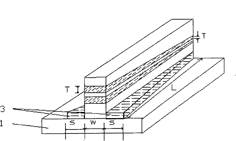
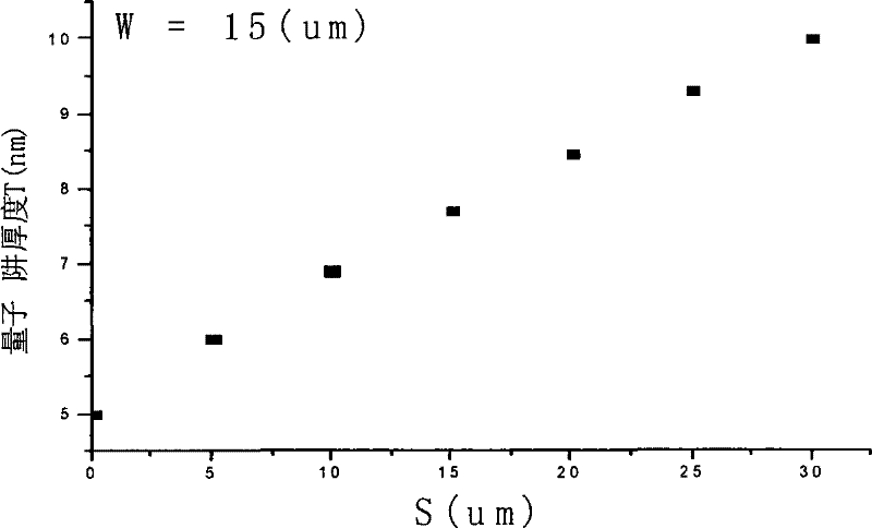
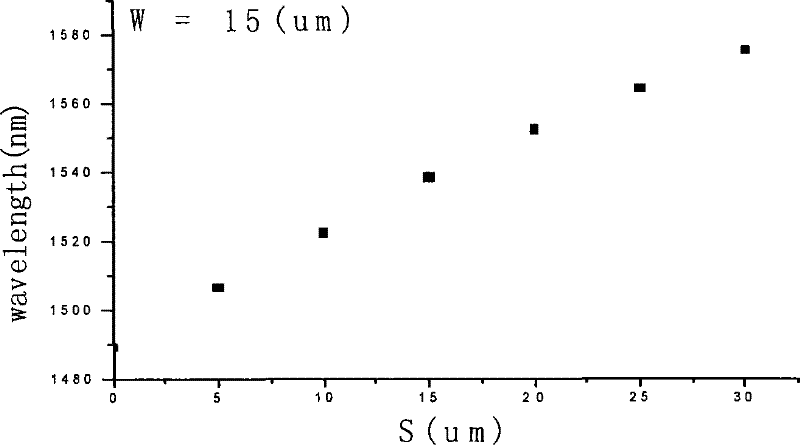
[0032] Figure 1 to Figure 3 is a schematic diagram of the principle of metal-organic chemical vapor deposition for selective area growth, in which, figure 1 It is a schematic diagram of metal-organic chemical vapor deposition for selective area growth provided by the present invention, figure 2 It is the curve that the quantum well thickness T of the selective region growth provided by the present invention varies with the silicon dioxide pattern width S, image 3 It is a curve of the quantum well bandgap wavelength of selective region growth varied with the silicon dioxide pattern width S provided by the present invention.

[0033] In...


PUM


Abstract

The invention discloses a wide-spectrum high-power semiconductor superradiance LED, which comprises a substrate and a gain medium positioned on the substrate, wherein the gain medium is formed by use of semiconductor material with an energy band structure and spatial variation. The invention also discloses a method for manufacturing wide-spectrum high-power semiconductor superradiance LED. As theinvention adopts the semiconductor material with an energy band structure and spatial variation as the gain medium, the radiation light of the superradiance LED has internal incoherence, so that wide-spectrum output can still be maintained under high output power.

Description

technical field [0001] The invention relates to the technical field of semiconductor superluminescent light-emitting diodes, in particular to a method for manufacturing a wide-spectrum and high-power semiconductor superluminescent light-emitting diode. Background technique [0002] Semiconductor superluminescent light-emitting diodes have a wide range of applications in fiber optic gyroscopes, optical test equipment, fiber optic sensing systems, fiber optic communication systems, and optical tomography. In the above applications, in order to reduce Reyleigh backscattering and improve system accuracy, it is necessary for superluminescent light-emitting diodes to have a wide spectrum. Due to the coupling loss, transmission loss, and splitting / combining loss in the actual system, some applications (such as distributed optical fiber sensing systems) also require superluminescent light-emitting diodes to have a large power output at the same time to improve the sensitivity of the...

Claims


Application Information

Patent Timeline
Patent Type & Authority Patents(China)
IPC IPC(8): H01L33/00
Inventor 赵玲娟张靖王圩
Owner INST OF SEMICONDUCTORS - CHINESE ACAD OF SCI
Learn More