Contact bonding pad for reducing parasitic capacitance and manufacturing method thereof

A technology for contacting pads and pads, which is applied in the direction of circuits, electrical components, and electrical solid devices, can solve the problems of reducing the effect of parasitic capacitance, not easy to add STI layers, and restrictions, so as to reduce the value of parasitic capacitance and increase the preparation process The effect of simple cost and preparation method

Active Publication Date: 2009-09-16
SHANGHAI HUAHONG GRACE SEMICON MFG CORP
View PDF0 Cites 8 Cited by
  • Summary
  • Abstract
  • Description
  • Claims
  • Application Information

AI Technical Summary

Problems solved by technology

[0005] but, figure 1 The STI region of the shown prior art that reduces the parasitic capacitance has obvious disadvantages: (1) due to the formation of the shallow trench isolation layer, a CMP (Chemical Mechanical Planarization, chemical mechanical planarization) process is required to complete, because the CMP has a castellated ( Dishing) effect, it is generally not easy to add an STI layer in the area directly below the pad metal layer; (2) Due to the characteristics of the preparation process of the STI layer, the height of the STI layer (depth in the Z direction) is limited, which will limit d The expansion of the value further limits the effect of reducing the parasitic capacitance

Method used


Image

  • Contact bonding pad for reducing parasitic capacitance and manufacturing method thereof
  • Contact bonding pad for reducing parasitic capacitance and manufacturing method thereof
  • Contact bonding pad for reducing parasitic capacitance and manufacturing method thereof

Examples


Embodiment Construction

[0026] In order to make the object, technical solution and advantages of the present invention clearer, the present invention will be further described in detail below in conjunction with the accompanying drawings.

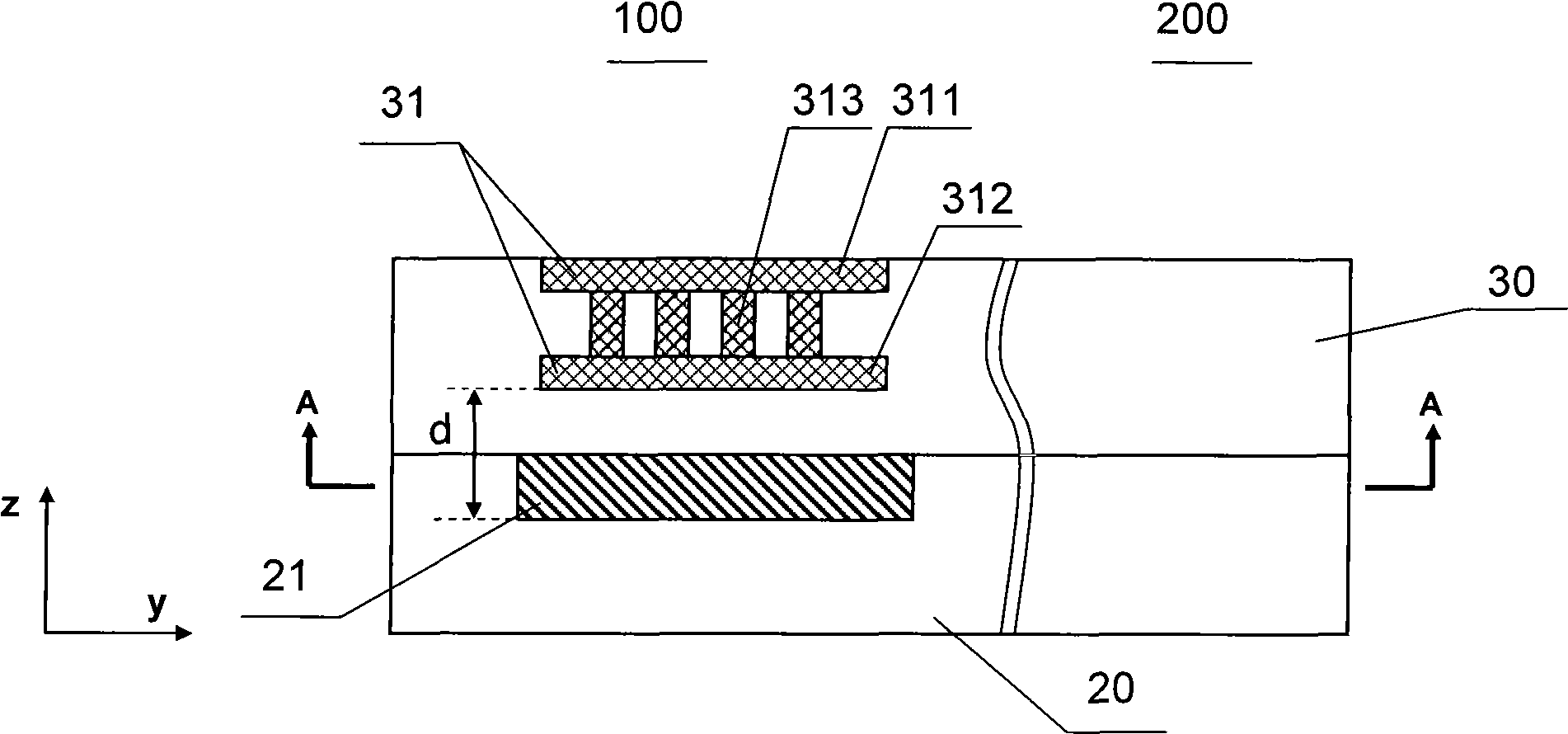
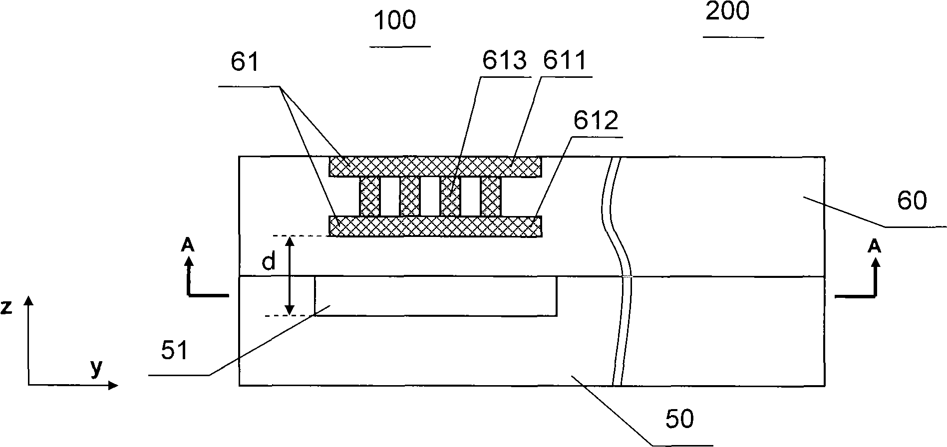
[0027] figure 2 Shown is a schematic structural diagram of the contact pad provided by the present invention. like figure 2 As shown, this embodiment provides a schematic diagram of a contact pad formed in the semiconductor substrate 50 and the interconnect structure layer 60, wherein the Z direction is a direction perpendicular to the upper surface of the semiconductor substrate. The interconnect structure layer 30 includes multiple metal layers, and the contact pad includes a pad metal layer 61. In this embodiment, the pad metal layer 61 includes a first layer of pad metal layer 611, a second layer of pad metal layer 612 And a hole (Via) 613 for connecting the first layer of pad metal layer and the second layer of pad metal layer, wherein the first layer of ...


PUM


Abstract

The invention discloses a contact bonding pad for reducing parasitic capacitance and a manufacturing method thereof, and belongs to the technical field of semiconductor manufacture. The contact bonding pad comprises a bonding pad metal layer, and a full exhaust layer area formed by alternative doping of a first type semiconductor and the second type semiconductor in the adjacent areas; the full exhaust layer area is formed in the semiconductor substrate and located on the upper surface of the semiconductor substrate below the bonding pad metal layer. The full exhaust layer area exbands the distance between the bonding pad metal layer and the semiconductor substrate and reduces the parasitic capacitance value of the contact bonding pad; meanwhile, the method for manufacturing the full exhaust layer area is simple, and does not increases the manufacturing processing cost of the contact bonding pad.

Description

technical field [0001] The invention belongs to the technical field of semiconductor manufacturing, and in particular relates to a contact pad with a fully depleted layer region and a preparation method thereof. Background technique [0002] In the packaging technology field of semiconductor manufacturing, after the integrated circuit is manufactured, the contact pad (Pad) formed on the surface of the interconnection structure layer is electrically connected to the internal circuit (internal circuits), which serves as a connection between the internal circuit and the external signal. The interface of the interface usually completes the electrical connection between the external circuit and the contact pad by means of bonding, that is, metal wires. The external signals include power signals, ground signals, and input / output signals. [0003] At the same time, as the feature size of the chip continues to decrease, the speed of the chip is getting faster and faster, and the req...

Claims


Application Information

Patent Timeline
Patent Type & Authority Applications(China)
IPC IPC(8): H01L23/482H01L21/60H01L21/8234
CPCH01L24/05H01L2924/14
Inventor 黎坡张拥华周建华彭树根
Owner SHANGHAI HUAHONG GRACE SEMICON MFG CORP
Why Eureka
Try Eureka