All-optical switch and design method thereof

An all-optical switching and design method technology, applied in optics, nonlinear optics, instruments, etc., can solve the problems of less obvious effect, high pump light intensity, singleness, etc., and achieve lower threshold intensity, high switching efficiency, easy to use. effect achieved

Inactive Publication Date: 2010-10-13
SUN YAT SEN UNIV
View PDF0 Cites 0 Cited by
  • Summary
  • Abstract
  • Description
  • Claims
  • Application Information

AI Technical Summary

Problems solved by technology

[0005] In order to solve the technical problems of high pump light intensity existing in the existing all-optical switch, and the single way to reduce the pump light power, the effect is not obvious, etc., the primary purpose of the present invention is to provide an all-optical switch design method, comprehensively utilizing the approach of reducing the pump light power, effectively reducing the threshold intensity of the pump light

Method used


Image

  • All-optical switch and design method thereof
  • All-optical switch and design method thereof
  • All-optical switch and design method thereof

Examples


Embodiment 1

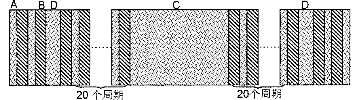
[0029] figure 1 Shown is the one-dimensional multilayer film structure containing three defect layers designed by the present invention, and its design process is specifically as follows:

[0030] Step 101: Incorporate a central defect layer C located in the middle of the multilayer film structure into the multilayer film structure in which the first medium layer A with high refractive index and the second medium layer B with low refractive index are alternately stacked, and then in the multilayer film structure Two side defect layers D are symmetrically doped into two ends far away from the center defect layer C; two adjacent first dielectric layers A and second dielectric layers B form a periodic dielectric film, and the side defect layer D and the center The defect layer C is generally separated by N periods of dielectric film to avoid mutual coupling between the defect layer D and the defect layer C, where N is greater than or equal to 6. The optical thickness of the cent...

Embodiment 2

[0036] figure 2 Shown is the one-dimensional multilayer film structure containing four defect layers designed by the present invention, and its design process is specifically as follows:

[0037] Step 201: symmetrically doping two symmetrical defect layers C located in the middle of the multilayer film structure into the multilayer film structure in which the first medium layer A with high refractive index and the second medium layer B with low refractive index are alternately stacked, and then In the film structure, two side defect layers D are symmetrically doped at both ends away from the adjacent symmetrical defect layer C; the adjacent first dielectric layer A and the second dielectric layer B form a periodic dielectric film, and the side The defect layer D is far away from the adjacent symmetrical defect layer C, and the side defect layer D and the symmetrical defect layer C are generally separated by N periods of dielectric film to avoid mutual coupling between the def...


PUM

PropertyMeasurementUnit
thicknessaaaaaaaaaa
wavelengthaaaaaaaaaa
thicknessaaaaaaaaaa

Abstract

The invention relates to a photon crystal all-optical switch and a design method thereof. The design method is as follows: a multilayer film structure is internally mixed with a center defect layer C or two symmetrical defect layers C and two side detect layers D, wherein N cycles of dielectric films are spaced between the side defect layers D and the defect layers C so as to avoid the mutual coupling of the side defect layers D and the defect layers C; then two detect modules are obtained through adjusting the optical thickness of the center detect layer C or adjusting the optical thickness of the two symmetrical defect layers C and the distance between the two symmetrical defect layers C, and then the optical thickness of the side detect layers D is set to obtain two defect modules withthe Q value ratio of about 2-4; the defect module with the low Q value is set to be a pump light channel, and the defect module with the high Q value is set to be a detection light channel. The invention realizes the all-optical switch with high switching efficiency larger than 90 percent through utilizing the bandgap characteristic of a photon crystal and mixing the nonlinear defect layers, and the needed pump light intensity is about 50 times lower than the condition with a single detect layer and same Q value.

Description

technical field [0001] The invention relates to the technical field of all-optical switches, in particular to a photonic crystal all-optical switch with a one-dimensional multilayer film structure and a design method thereof. Background technique [0002] A photonic crystal is a structure whose refractive index is distributed periodically with space. It has a photonic band gap and photon localization are the two most fundamental characteristics of a photonic crystal. Light waves with a frequency in the photonic band gap cannot propagate in a photonic crystal. The all-optical switch is an important integrated photonics device, which fully uses the interaction between photons and matter to realize the effective "on" and "off" control of the transmission process of the beam. It is used in optical communications, optical computers and fast optical devices. Information processing and other fields have very broad application prospects. Photonic crystals have a photonic band gap, ...

Claims


Application Information

Patent Timeline
Patent Type & Authority Patents(China)
IPC IPC(8): G02F1/35
Inventor 金崇君饶文媛
Owner SUN YAT SEN UNIV
Why Eureka
Try Eureka